

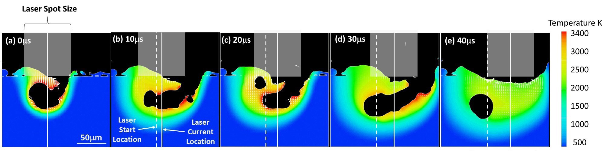
Remember when I told you a growing number of defect analysis tools are being developed and commercialized? As a reminder, some of the most common defects created during AM — and among the hardest to prevent — are keyhole formations. They appear during the laser powder bed fusion process.
When the lasers deposit too much energy too quickly into the melted metal or melt pool, tiny bubbles of vapor form and become trapped as the metal cools, weakening a part’s structural integrity. Because they form beneath actively printed layers, keyhole defects are hard to spot in real-time — but not impossible.
To address this issue – and on the heels of the PBF Process and Defect Analysis solution (PDA), the Johns Hopkins Applied Physics Laboratory (APL) in Laurel, Maryland have developed sensors that are fast enough to identify defects before they materialize.
“If we can identify defect formation while still in the melt state, then we have the opportunity to repair these imperfections before they result in performance-limiting flaws,” said Morgan Trexler, who leads APL’s Science of Extreme and Multifunctional Materials program. “We are working to make manufacturing processes more intelligent, which will inherently lead to more rapid manufacturing and trusted components.”
“We can identify rocks below the surface of rivers from space, not because we can actually see them directly, but because we can see rapids where the water flow is disrupted,” explained Steve Storck, project manager and chief scientist for manufacturing technologies in APL’s Research and Exploratory Development Department. “Similarly, if a pore is about to form in a part, then the thermal flow around it will be disrupted, which indicates a defect in the formation process. If we can measure that temperature and spectral anomalies accurately and rapidly, we should be able to tell if something is forming in, underneath or adjacent to the active melting location.”
The researchers hypothesized that these keyhole defects were occurring during transitional states. If they could pause the depositing laser just before the anomaly began to form, then the molten metal could cool long enough to settle and close the vapor depression, preventing bubble formation.
From Concept to Process
Credit: Johns Hopkins APL
The team first tested conventional sensors to see if they could identify the defect signatures fast enough, but ran into optical resolution and speed limitations. This prompted a collaboration with Mark Foster, an associate professor of electrical and computer engineering with the Johns Hopkins University’s Whiting School of Engineering, and several Whiting School postdoctoral students to enhance an APL-developed and patented sensor. Melding expertise in materials science, additive manufacturing, optical engineering and data science, they added photodiodes at multiple wavelengths and increased the sample frequency to measure high spatial- and temporal-resolution data on the melt pool and its dynamics, enabling them to gather the information needed to identify the early stages of a keyhole defect on a timescale that could enable real-time repair.
With the high-speed sensor up and running, the researchers developed a control framework that could communicate between the sensor and the laser and tell the laser to shut off when the melt pool got too hot and was likely to create a defect — all within 10 to 20 millionths of a second.
Continuing to draw on expertise from across APL, Storck and Pagán reached out to developer Mike Brown, who adapted a high-speed field-programmable gate array — essentially an integrated circuit that can be programmed to meet specific needs — that was originally designed for defense purposes, to seek missiles in the sky.
“One of the unique aspects of working at APL is the ability to leverage technology from areas that seemingly do not relate; for example, we can take the knowledge and expertise we apply to missile defense — responding to measurement inputs very quickly and making adjustments even faster — and apply it to additive manufacturing,” said Storck.
After integrating all the systems, the team successfully demonstrated the system’s ability to respond in a mere 952 nanoseconds — less than one microsecond, or faster than the blink of an eye.
“Those were great results, because at a minimum we need to measure at least twice as fast as what’s actually happening physically, so we can capture the peaks and valleys of the spectral response as it correlates to temperature,” Storck explained. “Our system can measure the spectral and temperature readings and respond 10 times faster than required based on simulations of keyhole formation.”
The team plans to incorporate artificial intelligence into the process to speed up the feedback loop and more accurately indicate where and how the defects are forming. Storck said this will enable real-time control and repair as APL works toward producing parts that can be trusted straight from the build.
Remember, you can post job opportunities in the AM Industry on 3D ADEPT Media for free or look for a job via our job board. Make sure to follow us on our social networks and subscribe to our weekly newsletter: Facebook, Twitter, LinkedIn & Instagram ! If you want to be featured in the next issue of our digital magazine or if you hear a story that needs to be heard, make sure you send it to contact@3dadept.com


