
In the manufacturing industry in general, most innovations evolve around the ability to produce large 3D printed parts. However, with the growing demand for miniaturized devices in electronics, biotechnology, automotive, and aerospace, there is an increasing interest in micro-additive manufacturing technologies. So, how big is the market of little parts?
The term micro additive manufacturing is often used interchangeably with 3D microfabrication or high-precision additive manufacturing while in reality, they are not exact synonyms. It’s fair to say that micro-AM can only be used interchangeably with micro-3D printing and the difference between the two terms reveals that AM refers to an industrial manufacturing context whereas 3D printing refers to a more “maker/prototyping” environment.
“3D microfabrication is a general term that describes all methods. The main part of this world would come from clean room fabrication such as lithography methods that are very common and widely used in MEMS manufacturing (this is a huge well-established market and the methods are very mature). There are a bunch of other 3D microfabrication methods, for example methods used for microfluidics, digital methods based on, say, e-beam litho, and many more.
High precision AM is probably not well defined and someone who has resolution of 100 microns would market it as high precision, so it very much depends on the context”, Jon Donner, the General Manager of Fabrica, a Nano Dimension company, states from the outset.
To provide context to the place of micro-AM technologies, let’s say that in 3D printing, a part is built first and described digitally by a dot array, where a dot, i.e., voxel, represents a minimum printing unit. The voxel size ranges from nanoscale to macroscale. Micro-3D printing processes therefore require the use of a micrometer or sub-micrometer scale voxel, which is pivotal for the fabrication of microproducts. The term micro-3D printing thus refers to the manufacturing of ultra-high-precision, tiny parts in shapes that cannot be achieved using microinjection moulding processes and other types of traditional manufacturing processes.
The present exclusive feature ambitions to discuss the various ways in which micro-AM challenges the traditional manufacturing status quo. It will shed light on:
- The fundamentals and different types of micro-AM technology.
- Main advantages and areas for improvement that may help this market move forward.
- The place of these processes in vertical industries, and in the medical and healthcare industries in particular.
Fundamentals and different types of micro-AM technology
An essential item that we look at, when we talk about AM on the microscale is “microns”. Microns are one of the elements that help to determine whether the process refers to micro-3D printing or just 3D printing. It goes without saying that the level of microns one can reach, varies from one technology to another.
When a part is measured in single-digit microns down to a layer thickness of 5 microns and a resolution of 2 microns, then we deal with a micro-3D printing process. Interestingly, some micro-AM processes can fabricate parts measurable in nanometers (nm), which is 1,000 times smaller than a micron. To better visualize these measures and picture how small the parts can be, one often keeps in mind that the average width of a human hair is 75 microns and a strand of human DNA is 2.5 nanometers in diameter.
“It is hard to say but in general we consider 10 microns and below as micro–AM. Specifically one can talk about pixel size or layer height or tolerance or repeatability. For sure, if all of these are in the 1-3 micron range then it is micro-AM”, Donner explains.
Just like there are several types of AM processes, there are also various types of micro-AM processes which include: fused filament deposition (FFD), direct ink writing (DIW), direct energy deposition (DED), direct light projection (DLP), laminated object manufacturing (LOM), electrohydrodynamic redox printing (EHDP), powder bed fusion (PBF), photopolymerization-based 3D printing (P3DP), and laser chemical vapor deposition (LCVD). The table below provides a summary of micro-3D printing methods in terms of material, process, fabrication rate, and resolution.
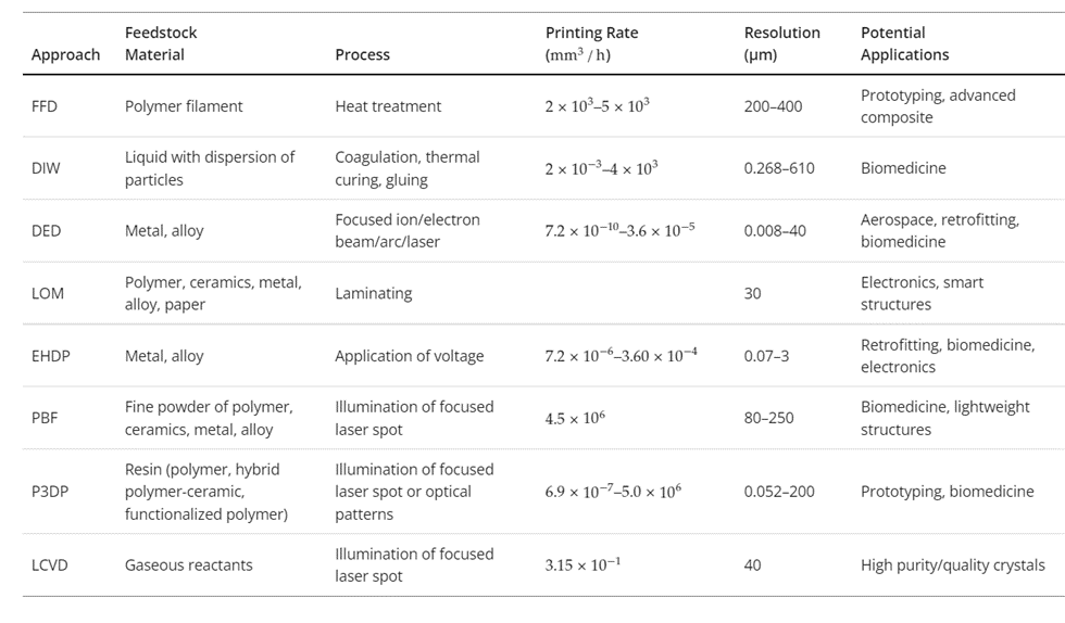
Micro-3D printing processes based on resin are currently the most acknowledged on the market due to their strength in resolution, quality, reproducibility and rate. Furthermore, DED and EHDP can achieve higher resolution. Nevertheless, the expensive cost and low fabrication rate associated to these processes limit their applications.
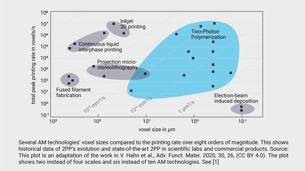
“The smallest feature sizes achieved by Two-Photon Polymerization extend far into the submicrometer range. This exceeds the capabilities of conventional 3D printing technologies. For example, Fused Deposition Modeling (FDM) or Selective Laser Sintering (SLS) are typically limited in their vertical and lateral resolution. The achieved feature sizes are in the range of several hundred micrometers. Resin cross-linking technologies, such as stereolithography (SLA) and digital light processing (DLP), achieve a slightly higher precision than the above-mentioned AM technologies (in the range of 5 to 10 micrometers).

However, they still have limitations in realizing small high-precision parts or structures due to their limited resolution. In contrast to these methods, 2PP enables the manufacturing of minimal feature sizes down to 100 nanometers. The printing rate of 2PP-based 3D printing processes is at least competitive with digital light projection (DLP) stereolithography. One general metric for print speed refers to the rate in voxels printed per second and is an indicator of how digital information is converted into solidified material” Jörg Smolenski, Business Development Manager at Nanoscribe adds.
According to research, the development of novel optical methods has led to the advancement of micro-AM processes, photopolymerization-based printing processes in particular. According to experts, using a light source with shorter wavelengths, e.g., UV beam, and an objective with higher NA (Numerical aperture) enables to achieve a higher resolution – which is often one of the most highlighted challenges to overcome in micro-AM.
The optical method renders a firmer connection of adjacent voxels as opposed to other approaches based on heat treatment and laminating. The post-processing step, such as photo-curing, also contributes to the quality of 3D printing parts. Lastly, the laser spot or optical pattern that processes the feedstock facilitates the stability and reproducibility as a result of the non-contact approach between the processing region and the illumination system, the report reads.
That being said, the most widely known micro-AM processes include DLP, Microstereolithography (µSLA), Projection Microstereolithography (PµSL), Two-Photon Polymerization (2PP or TPP), Lithography-based Metal Manufacturing (LMM), Electrochemical Deposition and Microscale Selective Laser Sintering (μSLS).
Direct Light Projection (DLP) Technology
DLP technology enables to achieve repeatable micron levels of resolution by combining DLP with the use of adaptive optics. One of the main differences with SLA with which it is often said to be very similar to, is that SLA requires the use of a laser to trace a layer, while DLP uses a projected light source to cure the entire layer at once.
Microstereolithography (µSLA)
Also based on a light-induced layer-stacking manufacturing, micro-Stereolithography (MPuSLA) is used to build physical components by exposing a photopolymer resin to an ultraviolet laser. If you are familiar with the utilization of a resin 3D printer, leveraging an µSLA machine shouldn’t be a problem.
Projection Microstereolithography (PµSL)
PµSL is a high-resolution (up to 0.6 μm) 3D printing technology based on area projection triggered photopolymerization, and capable of fabricating complex 3D architectures covering multiple scales and with multiple materials. Machines based on this process are often said to combine the benefits of both DLP and SLA technologies. The process rapidly evolves due to its affordability, accuracy, speed and its ability to process polymers, biomaterials, and ceramics.
Lithography-based Metal Manufacturing
As extensively described in this conversation with MetShape, this process can fabricate tiny metal components using some of the same principles of photopolymerization. After a homogeneous dispersion in a light-sensitive resin, the metal powder is thereafter selectively polymerized by exposure with blue light. The green parts should undergo a sintering process in a furnace before being ready for use.
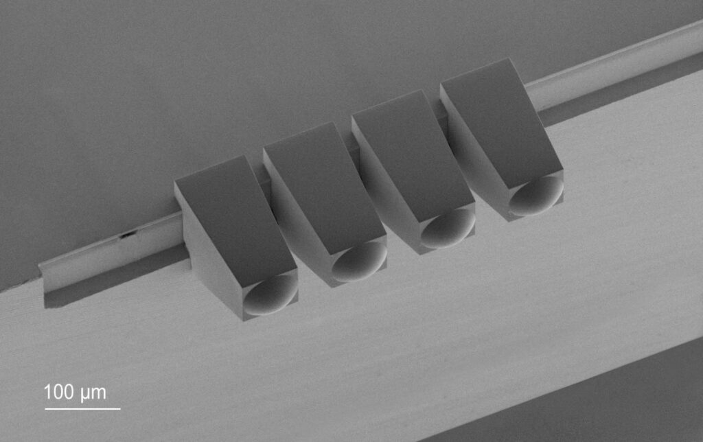
Two-Photon Polymerization (2PP or TPP)
This process is often said to provide the highest accuracy among micro-3D printers. The manufacturing technology consists in the use of a pulsed femtosecond laser to trace 3D patterns in the depth of the vat of special photosensitive resin. Nanoscribe’s Jörg Smolenski provides an easier explanation of the process:
“2PP unfolds its full potential at the interface between maskless lithography and high-precision additive manufacturing. The process belongs to a family of AM technologies, in which light is used to cure a liquid photoresin to create a digitally defined structure. The combination of 2PP with a robust 3D printing workflow enables multiple manufacturing scenarios. 2PP is a direct laser writing approach and works without the need of the costly generation of masks and the use of multiple lithographic steps for 3D and 2.5D microstructures. 2PP advances the microfabrication of parts on flat substrates at wafer level, but also enables to directly print complex structures on pre-existing patterns and topographies, e.g., on optical fibers, photonic chips and inside sealed microfluidic channels. 2PP requires polymer printing materials and the dedicated photoresins for an easy handling and best possible resolution and shape accuracy as well as tailor-made for different applications. This allows to benefit from submicron features, overhanging elements, optical-quality surfaces, high-speed mesoscale fabrication, biocompatibility or high refractive index. High-precision 3D printing based on Two-Photon Polymerization is ideal for rapid prototyping of application designs to realize biomedical devices, microoptics, microelectromechanical systems (MEMS), microfluidic devices, photonic packaging (e.g. PIC), surface engineering projects and many more. Wafer handling capabilities make batch processing and small series production of 3D microparts easier than ever.”
Electrochemical Deposition
Electrochemical Deposition is one of those rare micro-3D printing technologies that does not require any post-processing. The process works with a little printing nozzle called iontip, and which is immersed in a supporting electrolyte bath. A regulated air-pressure pushes a liquid containing metal ions through a microchannel inside the iontip. At the end of the microchannel, the ion containing liquid is released onto the print surface. The dissolved metal ions are then electrodeposited into solid metal atoms. The latter grow thereafter into larger building blocks (voxels) until the part is formed.
Microscale Selective Laser Sintering (μSLS)
Also called selective laser sintering (SLS) on a micro scale, this powder bed fusion-based additive manufacturing involves coating a substrate with a layer of metal nanoparticle ink and drying it to generate a homogeneous nanoparticle layer. Thereafter, a laser light that has been patterned using a digital micromirror array sinters the nanoparticles into the desired patterns. The process is then repeated until the part is created.
So, what are the decisive factors to consider when choosing one technology over another?
A quick search on the market players developing micro-AM processes reveals that the market is still nascent. As a matter of fact, we usually found that only one or two players develop each process.
Nevertheless, some of the key items that could tilt the balance in favour of one technology, may include materials (obviously), robustness, speed, quality and size.
“First and foremost, the materials each technology enables are key factors in any choice. Second is how robust and precise the system is and specifically the speed and tolerances you can reach. Another critical factor is the size you can print in the bounding box. Finally, throughput and repeatability are key decision points”, Jon Donner comments.
Needless to say that each process cannot deliver the same advantages or have the same limitations. Sometimes, the choice of the user will be based on the sought advantages for a given application or the limitations to avoid for another one. For example, “Two-Photon Polymerization is a new technology known in the industrial context primarily for its quality and high precision. Similar to DLP, it uses light to crosslink a photosensitive resin to fabricate nano-, micro- and mesoscale structures, but it does so only in a very small volume of significantly less than 1 micrometer in diameter. 2PP is said to be slow when it comes to micro- and mesoscale structures. This has changed recently with the advance of new processing technologies such as Two Photon Grayscale Lithography (2GL ®) and the combination of higher power laser that have come on the market and improved hardware such as stages and scanners. Other conventional AM technologies such as DLP, SLA, and Projection Micro Stereolithography (PµSL) can only fabricate larger structures with less filigree feature details in the range of several micrometers. These technologies are clearly suitable for some microfabrication tasks. However, they encounter geometric limitations when it comes to high- resolution (<1 micrometer) 3D Microfabrication. Resolution and design geometry are limited due to the inherent direct illumination with UV light. 2PP provides the freedom of full 3D design to fabricate freeform, porous and even organic 3D geometries with excellent shape accuracy in the submicrometer to millimeter range. The inherent geometric limitations associated with subtractive methods are overcome with 2PP due to the additive approach.”, Smolenski states, reflecting on the advantages and limitations of some of the aforementioned technologies.
In general, here are the key benefits and areas for improvement we will keep in mind when exploring micro-3D printing technologies:
| Benefits | Areas for improvement |
| Low cost: compared to micro-injection moulding processes, leveraging a micro-3D printing process remains affordable for those who are looking to achieve prototypes or serial production. | Materials: like in traditional AM technologies, materials remain the hurdle that continuously requires advancements. “As new materials are developed, as yields increase, we will see many new areas where micro-AM will be applied”, Donner comments. |
| Greater design possibilities: As any 3D printing process, micro-3D printing allows its user to benefit from design freedom. | “A challenge in the fields of photonic integration, optical computing and data communications is to advance the alignment and packaging of photonic components. Specialized hardware- and software- based printing solutions can in turn enable efficient microoptical coupling. That’s why we have recently introduced and will continue to develop precisely aligned 3D printing on optical fibers and photonic chips”, Smolenski adds. |
| Speed: it’s quite captivating to see how fast one can manufacture a small part compared to the same part manufactured via traditional manufacturing processes. | Time: Micro-AM remains a relatively new entrant on the market and as seen with any new technology, it takes time to convince companies to use it. |
The place of these processes in vertical industries, and in the medical and healthcare industries in particular.
As stated in the very first paragraph, micro-3D printing first found its use in the electronics industry. With the advancements of miniaturized microproducts, the technology increasingly positions itself as the way to go for other applications.
To date, “all industries that deal with small and precision parts are applicable. Making small parts traditionally has always been expensive, and Micro-AM is now delivering much cheaper and accessible solutions. In miniaturization, control over form factor is critical and enables a “next level” of miniaturization. Specifically: electronics, optics, semicon, medical devices, medical tooling, micro-injection molding, microfluidics, sensors, and then these applications of course are found in auto, aerospace, consumer goods, etc.” Fabrica’s expert points out.

Furthermore, medical device research is the strongest field where micro-AM can reveal its potential (Fabrica’s opinion).
“As micro-AM is a “new” field it is currently only used for prototyping. But we see many opportunities. Some examples are micro-needles, parts for small blood vessels like blood clot-related tooling, tooling for ophthalmology, and many more. We are also seeing many miniaturized medical devices”, Donner notes.
Nanoscribe goes one step further and highlights the fact that it has recently made 2PP accessible for high-precision 3D bioprinting:
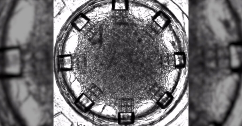
“High-precision 3D bioprinting enables to create advanced microenvironments for tissue engineering, custom scaffolds for cell studies, and many other innovative biomedical applications where precision, speed, material diversity, and sterility matter. In cell cultivation or cell seeding applications, microstructures are first printed using a material such as hydrogels or one of Nanoscribe’s biocompatible IP Photoresins. After printing, the structures are rinsed and cells are seeded onto the structures. Typically, the substrates are kept in incubators to monitor cell behavior over time. Cell seeding is the most common technique to combine 2PP microfabrication with cell research. Moreover, the dedicated high-precision bioprinter Quantum X bio covers biomedical applications like customized microfluidic elements and microneedle arrays or microrobots for drug delivery. Connecting the micro to the macro world, 3D structures can be placed intuitively and with highest precision into microfluidic channels or wells by simply tapping on the machine’s touchscreen.”
Lastly, 3D Microfabrication can bring life science research a big step closer to the concept of regenerative medicine for the curing of diseases in this field. For example, Boston University scientists contributed to this goal with a microfluidic heart-on-a chip platform fabricated by Two-Photon Polymerization (2PP). The research team developed a soft and mechanically active cell culture platform to study heart muscle tissue in a customizable 3D microenvironment. This multifunctional toolbox allows cardiac tissue to be grown in a 3D environment and its self-assembly to be observed at cell attachment sites on the vertical walls of the chip. An integrated electronic sensor measures the forces generated by the contractions of the cultivated heart cells. Furthermore, the researchers integrated a mechanical actuator into the chip to passively stretch the cultivated tissue. With this actuator, the scientists investigated the influence of constant and dynamic mechanical strain on the heart tissue. The scale of biological tissue and submicron resolution of 2PP-based 3D printing are perfectly suited to mimic the natural environment. Coupled with the development of biocompatible materials for 2PP-based 3D printing, many other exciting applications in tissue engineering, cell biology and regenerative medicine can be expected, Nanoscribe’s expert concludes.
Concluding thoughts
Micro-AM’s ability to solve “small” problems can definitely have a big impact across industries. There might be several processes for microscale 3D printing but two photon polymerisation, projection μSL, and DLP would currently be the most promising. This field of activity currently faces some of the main challenges we observed with traditional AM processes, and as observed in that market, one of the fastest ways to drive this niche market forward is by improving process efficiency so that the methods allow for more applications, and obviously by putting the machines to work through collaborations.
Resources
This dossier has first been published in the May/June edition of 3D ADEPT Mag.
This exclusive feature has been written thanks to several external resources and main contributions from industry insiders. Exclusive interviews have been conducted with Fabrica, a Nano Dimension company as well as Nanoscribe.
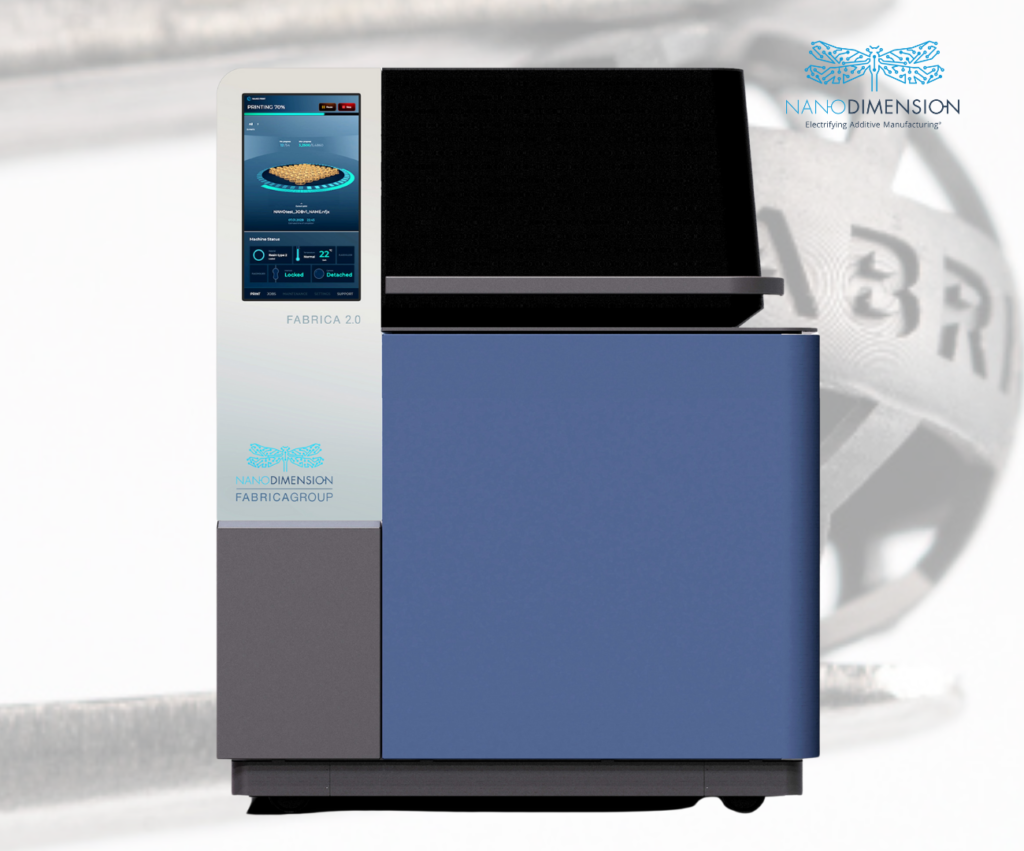
Fabrica 2.0 by Nano Dimension is a leading-edge hardware and software solution for Micro-AM delivering 1-5 micron additive layers for high precision in miniature parts. Fabrica 2.0 enables in-house part prototyping without the need for costly tooling and setup, delivering parts within hours using a digital light protection technology. Fabrica 2.0 currently works with the Precision N-800 ABS-like material and the Performance N-900 reinforced composite material for harsh and high temperature environments.
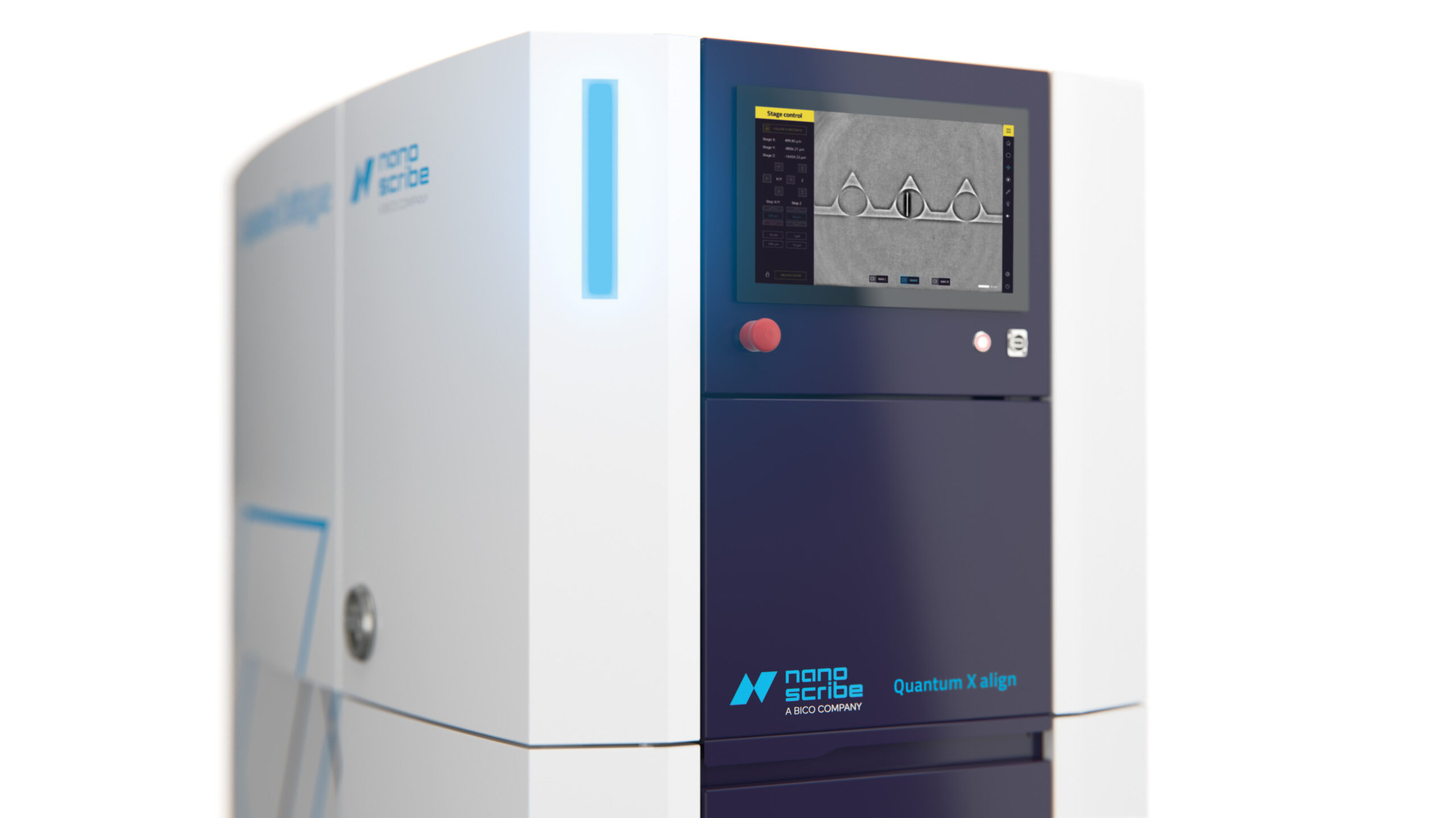
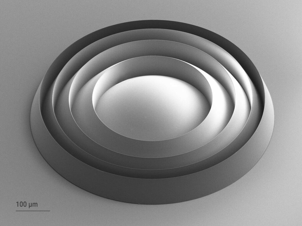
Nanoscribe works closely with high-tech companies and partners from research institutes and universities to continuously advance 3D Microfabrication, shaping pioneering research fields and industries. With the recently introduced Quantum X align, Nanoscribe thus offers a novel industrial solution for photonic packaging by precisely aligned 3D printing on optical fibers and photonic chips. This reduces coupling losses by mode field matching at the component level instead of the chip level. High- precision 3D printing with automatic alignment in nanoprecision advances the fabrication of microoptical components directly on photonic chips and fiber cores. The spatial orientation of the fiber cores or photonic chips is automatically detected, and freeform microoptical components or diffractive optical elements (DOEs) are printed directly in place, facilitating optimized optical coupling on photonic platforms. Nanoscribe’s proprietary Two-Photon Grayscale Lithography (2GL ®) significantly speeds up the high-precision microfabrication of 2.5D structures for optical applications, such as prototyping or mastering of freeform microoptics, microlens arrays, and multilevel diffractive optical elements with the highest shape accuracy and optical-grade surfaces (Ra ≤ 5 nanometers). To scale up production even further, the combination of 2GL mastering with replication technologies comes into play. With nanoimprint lithography (NIL) and injection molding (IM), Nanoscribe has already piloted two reliable and proven replication strategies together with EV Group and kdg opticomp.
This allows to benefit from short design iteration cycles of the 2GL additive manufacturing process and then via replication to move optical-grade microoptics manufacturing into mass production.
Projection micro stereolithography based 3D printing and its applications, IOP Publishing Ltd on behalf of the IMMT.
Bert Huis in ‘t Veld, Micro additive manufacturing using ultra short laser pulses
Wei Lin, Dihan Chen, and Shih-Chi Chen, Emerging micro-additive manufacturing technologies enabled by novel optical methods V. Hahn, P. Kiefer, T. Frenzel, J. Qu, E. Blasco, C. Barner-Kowollik, & M. Wegener (2020). Rapid Assembly of Small Materials Building Blocks (Voxels) into Large Functional 3D Metamaterials. Advanced Functional Materials, Vol. 30, June 2020, 1907795.


