

“ALD rings are not necessarily the leading application of Additive Manufacturing (AM) in the semiconductor industry, but they are the most innovative,” Johannes Homa, CEO and founder of Lithoz, told 3D ADEPT Media. “Their significance lies in how well they demonstrate AM’s value in addressing key challenges of semiconductor fabrication.”
That bold statement immediately raised a dozen “why” questions in my mind. Fortunately, Homa took 50 minutes out of his Wednesday shift to clarify these gray areas.
I was genuinely pleased that, for this traditional annual catch-up, we focused on something other than healthcare. Don’t get me wrong—Lithoz’s ceramic 3D printing technology continues to achieve remarkable results in the healthcare sector. In fact, a recent study showing a 92% total success rate with the Lithabone material has further strengthened the credibility of the company’s technology in that field. But with semiconductor unit sales reaching a record 1.15 trillion shipments in 2021 alone, it’s clear that other niche markets also deserve our attention—particularly to understand how AM can tap into this opportunity.
In a recent dossier on “How AM and the semiconductor industry can help each other” (January/February edition of 3D ADEPT Mag; pp 6-8), global designer and manufacturer of semiconductor process equipment Veeco Instruments explains that the supply chain issue (illustrated through Moore’s law) led to the exploration of AM as a production candidate in the semiconductor industry. To decrease reliance on foreign suppliers, for instance, countries like the USA, which would like to enhance supply chain resilience, would need to address the challenges (long lead times, increased waste & cost) of current methods of fabrication in the field. That’s exactly where AM comes into play. To understand the potential of AM in this sector, my conversation with Homa focused on ALD rings.
 Why ALD rings?
For those who are new to this topic, keep in mind that ALD rings are consumable parts used in Atomic Layer Deposition (ALD) equipment — ALD is a specific type of deposition used to apply thin layers of material (metals, insulators, semiconductors) onto the wafer surface. Deposition, on the other hand, is one of the 6 critical steps used to manufacture a microchip; the other being photoresist, lithography, etch, ionization, and packaging.
If an ALD ring malfunctions, is misaligned, or causes non-uniform deposition, it can contaminate the wafer, cause film thickness variation, or result in wafer rejection (scrap).
“The ring controls the flow of gases used to deposit ultra-thin layers of material (often just a single atomic layer thick) onto the wafer surface. It plays a crucial role in the whole machine, especially in the deposition process and in the etching and buildup of materials during chip fabrication. Traditionally, this was a very time-consuming process because etching and deposition occurred in separate steps, requiring the wafer to be moved between different machines or the chamber conditions to be changed repeatedly, which slowed down throughput.
What we learned from the new FALP (Fast atomic layer processing) developed by Dr. Stephan Wege from Plasway, is that innovations in ALD equipment design—beyond the ring itself—allow etching and deposition to happen within the same machine and process cycle without breaking vacuum or swapping tools.
Historically, these rings were made from metals with nozzles designed to evenly distribute gases inside the chamber. The only thing is, metal rings often face two major challenges: corrosion resistance and ensuring consistent gas distribution. Since ALD works at the scale of single atomic layers, reproducibility in manufacturing these rings is therefore critical,” Homa explained.
To prevent tiny variations from significantly affecting film quality and overall yield, it’s crucial to explore AM as an alternative production candidate for these ALD rings.
Why Lithoz’s lithography-based ceramic manufacturing (LCM) in particular?
A few AM processes have made it to the short list of manufacturing techniques that can produce ALD rings for semiconductor applications. They include laser powder bed fusion (LBPF), Electron Beam Melting (EBM), Binder Jetting, SLA, and LCM.
However, understanding the potential LCM brings to the table should not be done in comparison with these processes. My conversation with Lithoz’s CEO helped me identify three performance areas where the company’s flagship technology shines: Manufacturing capabilities, time, and cost.
Manufacturing capabilities
As a reminder, Lithoz’s flagship product is a process where ceramic particles are dispersed in a photosensitive resin. This dispersion is thereafter solidified by light layer-by-layer to form a part. Then the part undergoes a sintering process to develop its ceramic properties and can be used for its final purpose.
“Where we are most active is in the core functional zones of the semiconductor equipment — the areas where critical processes like etching, material deposition, and wafer cleaning take place. These zones are exposed to extremely harsh chemical and thermal environments. That’s precisely where high-performance ceramics, and by extension LCM (Lithography-based Ceramic Manufacturing), come into play,” the CEO points out, speaking of ALD ring applications.
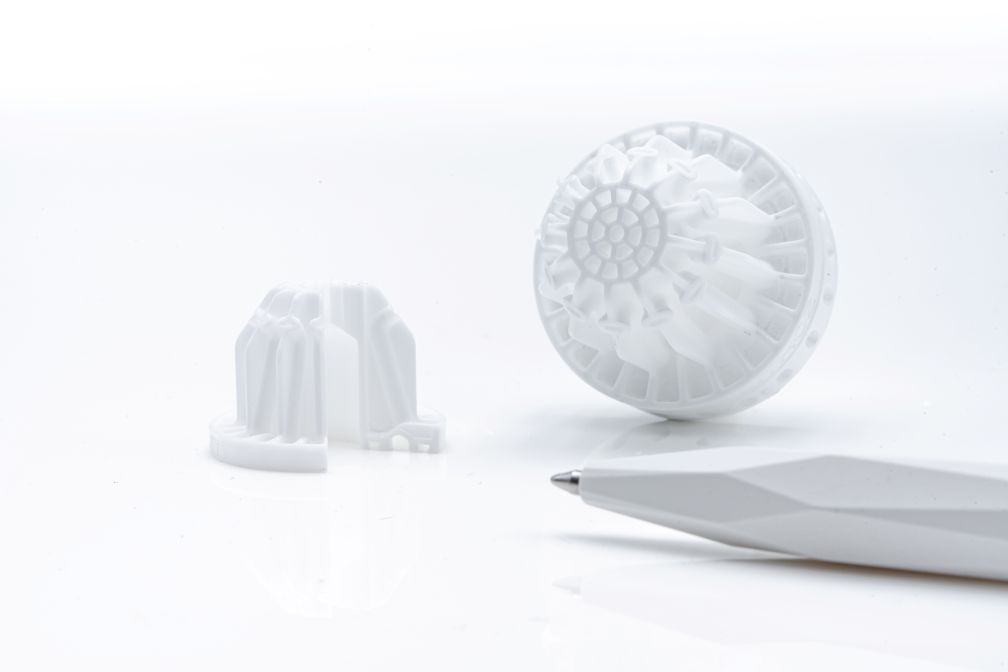
To clarify, ALD rings manufactured using LCM are designed for use in the core processing zone of the ALD equipment, where etching, depositionhappen in a plasma environment. This area is exposed to aggressive chemicals, high heat, and vacuum conditions during etching and deposition steps. Conventional manufactured metal versions of ALD rings often fail to deliver performance due to corrosion, inconsistent gas flow, and thermal fatigue.
Using LCM, manufacturers can produce complex ceramic ALD rings with internal channels for precise gas distribution, maintain tight tolerances, and repeatability needed for atomic-scale layer control.
“While alumina remains the key material for manufacturing ALD rings, aluminum nitride (particularly for components like heating plates), YAG, yttria, and silicon carbide are other technical ceramics that can be explored for semiconductor applications,” Homa emphasizes.
Time
As you may know, AM is often praised for enabling faster production compared to conventional manufacturing techniques. However, when I refer to “time” as a key performance indicator in this context, I’m talking about how a 3D printed ALD ring helps semiconductor manufacturers improve operational efficiency. Once installed in semiconductor manufacturing equipment, the 3D printed ALD ring can increase productivity by up to three times compared to conventional metal rings. Most notably, it extends uptime from just 1 month to 9 months. Additional testing reveals that today, uptime has increased even further.
Cost
It’s hard to truly weigh the massive financial implications that can result from improvements in process uniformity for ALD rings in particular. To ensure a more realistic discussion, let’s consider 3D printed parts that are produced for a semiconductor manufacturing machine.
A 3D printed part’s 0.01% change in design can improve wafer uniformity, reduce rework, or extend tool uptime. It could impact throughput or reduce scrap — all of which translate directly to money saved.
The question is, how much?
Well, semiconductor fabrication plants operate 24/7 with high costs per minute of downtime (sometimes $100,000+ per hour). A 0.01% design improvement in a 3D printed part can help save up to $240K/day if that change affects process-critical performance, if it’s scaled across many tools, and if it addresses a high-cost pain point like downtime or yield loss.
For this specific application, Homa told 3D ADEPT that “up to 100 CeraFab System printers can be synchronized, independent of their location, qualifying this rapidly scalable technology as a valuable factor in the reshoring of semiconductor production.”
Other applications of AM in the semiconductor industry

Although ALD rings showcase the value of Lithoz’s LCM technology in terms of performance, time, and cost within a mission-critical environment, they are just one part of a growing portfolio of applications that are collectively redefining how semiconductor equipment and tooling are designed, produced, and maintained. In the market, we’ve already seen the technology become central to certain vertically integrated businesses—particularly through the production of heat exchangers. Homa also cited gas equalizers, gas distribution nozzles, heating and cooling platesas additional key applications where AM can unlock new potential.
These are just the first steps in a broader journey for Lithoz in the semiconductor sector. Stay tuned as we uncover what’s coming next from the Austrian company.
This content has been created in collaboration with Lithoz. Johannes Homa’s words have been edited for brevity and clarity. Discover more about Lithoz’ technology capabilities in these “FOCUS” articles.


