

Archive — Published in 2019, this feature describes technologies and equipment from that period. Simon Fried’s remarks concern the 2018 market; cited technical parameters do not describe every current machine.
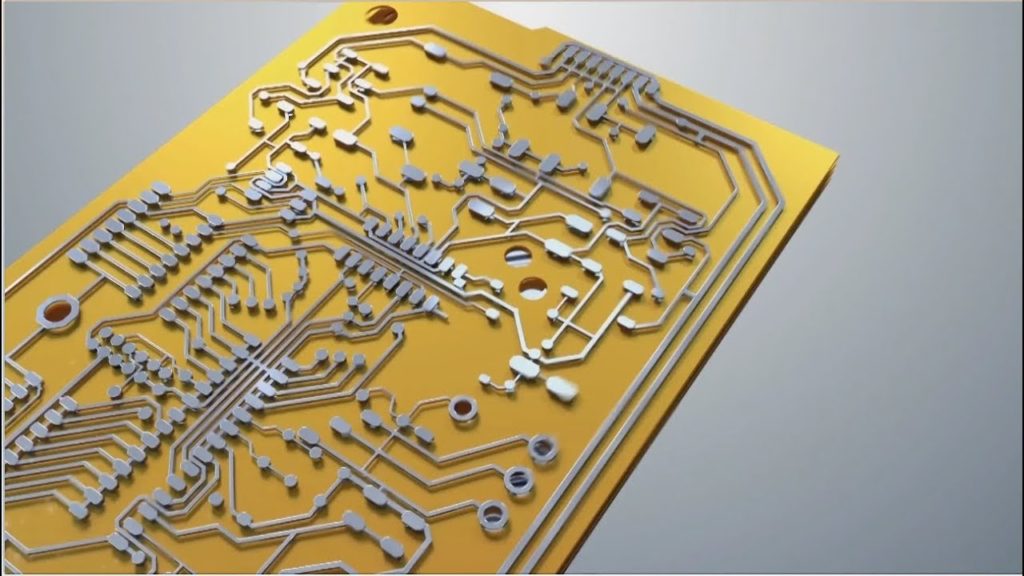
3D Printed electronics is one of the young areas of application of additive manufacturing. In his analysis of the 3D printing market in 2018, President Nano Dimension USA, Inc. Simon Fried, told us that the evolution of this market “has been similar to how traditional additive mechanical manufacturing evolved. The companies leading the adoption of additive manufacturing are the same kinds of industries that are now making strides in the direction of additive manufacturing of electronics — including aerospace, defense and R&D organizations. During 2018, this revolutionary area of 3D printing continued gaining traction, its impact will be felt in products, production systems and design-flows.” This statement left a great number of unanswered questions among additive manufacturing professionals, especially engineers from engineering offices. We have decided to tackle them in this segment.
Printed electronics includes depositing functional inks on a substrate. Screen, inkjet, flexographic or gravure printing can produce features for circuits, sensors or RFID tags. Required performance and cost depend on the application; neither is necessarily low.
However, the recent development of tools for AM has raised three main challenges in efficiently applying 3D Printed electronics. For Christoph Völcker from the Innovation Lab – AM Würth Elektronik eiSos GmbH & Co. KG, those main challenges are materials, techniques (hardware) and data.
Materials
Combining functional materials with three-dimensional geometries can enable circuits on non-planar surfaces or components embedded in a structure. It does not mean that every electronic component is itself printed.
Dielectrics provide insulation; conductors carry current. In the 2017 study by Flowers and colleagues at Duke, Hatchbox PLA and ColorFabb bronze-fill PLA served as dielectrics, while Electrifi, Black Magic 3D graphene PLA and Proto-pasta carbon-black PLA were conductive. Their resistivities differ; these composites are not equivalent to bulk copper.
Those various materials raise the challenge of cross-contamination during the fabrication. Indeed, it is difficult to combine two different filaments during the printing process. According to a research from Duke University (in the USA), “cross contamination of conductive materials will result in either shorting between conductive traces, or in the interruption of a conductive trace with non-conductive materials.”
Although several 3D printers with multiple nozzles can be found on the market – understand FDM 3D Printers – most of them are not able to prevent cross-contamination whereas “typical multi-material 3D printers use two separate nozzles at the same Z height, but this method leaves the inactive nozzle in a position where it is likely to scrape across the printed surface and cause cross-contamination”, explains the research from Duke University. According to experts, one approach to solve this issue is to extrude multiple materials through the same nozzle.
This observation concerns the machines tested in the 2017 study. The authors also describe purge limitations with a shared nozzle and use retractable nozzles in their own demonstrator.
This challenge is observed when 3D printed electronics is applied with professional 3D printers. At the industrial level, Nano Dimension, one of the companies that specializes in 3D printed electronics, mentions the need of more material options to produce high-complexity and high-functionality parts. While comparing all 3D Printing materials used in the AM industry, Simon Fried told us: “Polymers are getting stronger and a wider range of metals are now printable. For electronics, additional functional aspects such as dielectric constants and losses are paramount.”
Hardware
Nano Dimension, Optomec, BotFactory and Voxel8 are the examples selected for this historical overview. This is neither an exhaustive supplier inventory nor a current catalogue.
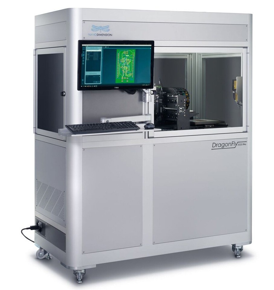
Described in the 2017 study, Nano Dimension’s 3D printer DragonFly 2020 produces multilayer printing of conductive traces using an inkjet technique at a lateral resolution of nearly 30 µm. Experts from Duke University stated that it is time consuming to develop novel electronic inks for ink-jet processes, not to mention the difficulties encountered. This is mainly due to the need to adapt the surface tension and viscosity (8–12 cp) of the ink to obtain a desired droplet size (∼30 µm) and reproducible jetting characteristics. Furthermore, “clogging can be an issue if the size of the particles or the amount of solids in the ink is too high”.
Optomec on its side, has developed the Aerosol JetTM process. The 3D printer enables the deposition of polymeric and metal inks for sensors. The process is a non-contact one, compatible with a wide range of conductive, insulating and resistive materials. The 3D printer has already enabled the production of conformal sensors, low loss passives and antennas for on-chip and off-chip electronics.
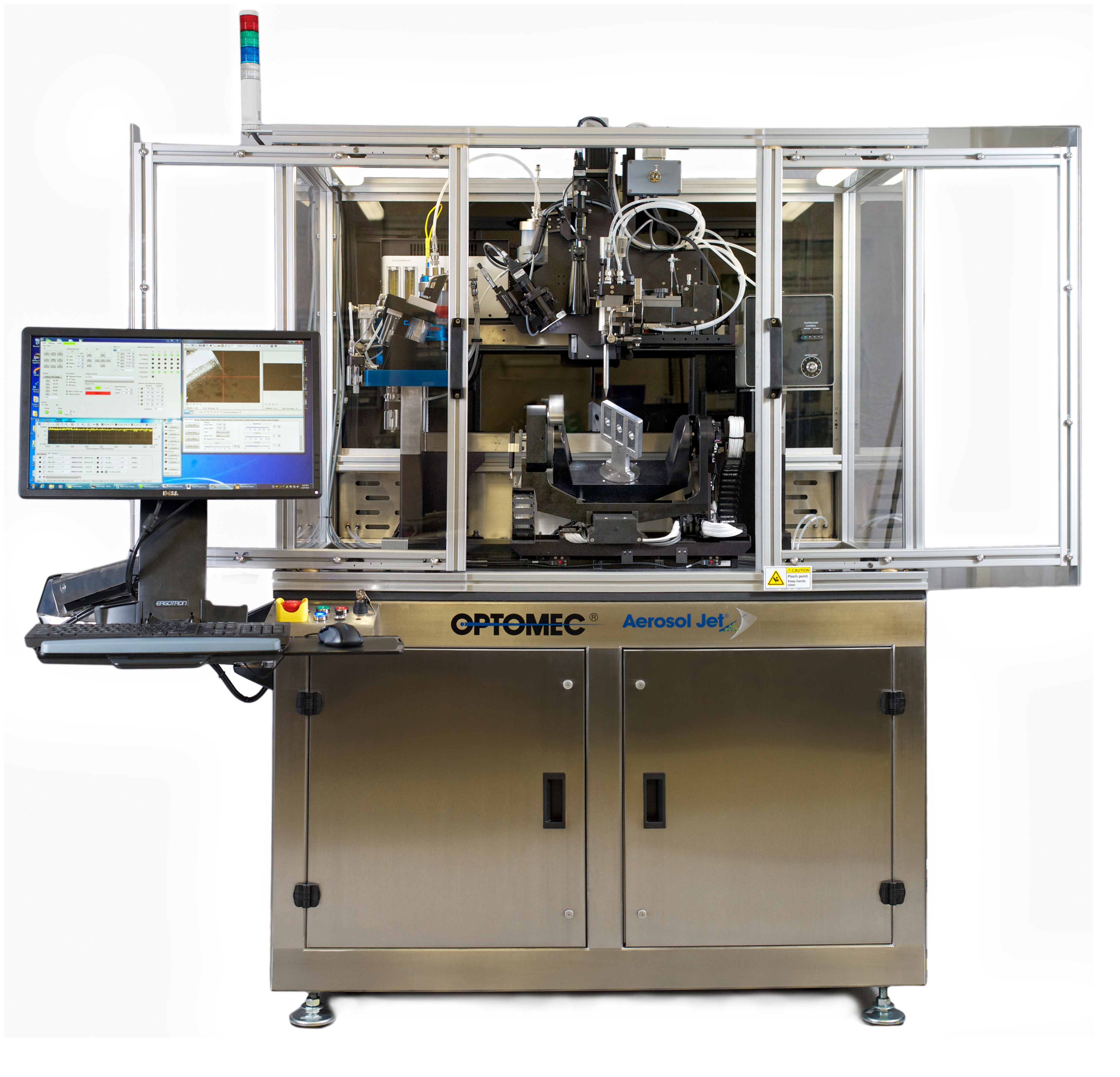
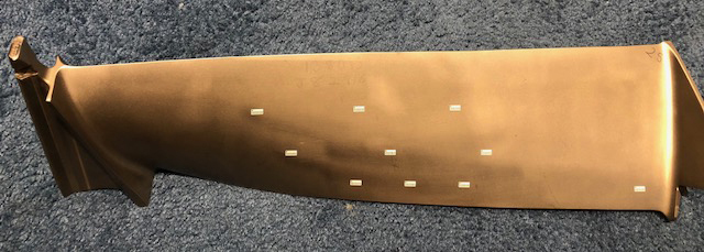
In Aerosol Jet, sheath gas surrounds and focuses the aerosol through a nozzle. It limits contact with the walls and associated clogging risk; it does not physically replace the nozzle.
BotFactory developed the Squink and SV2 circuit printers. The latter is a desktop PCB printer. It is, as per the company’s words, “capable of printing multilayer circuits, dispensing paste onto pads, and pick-and-placing components onto the board”.
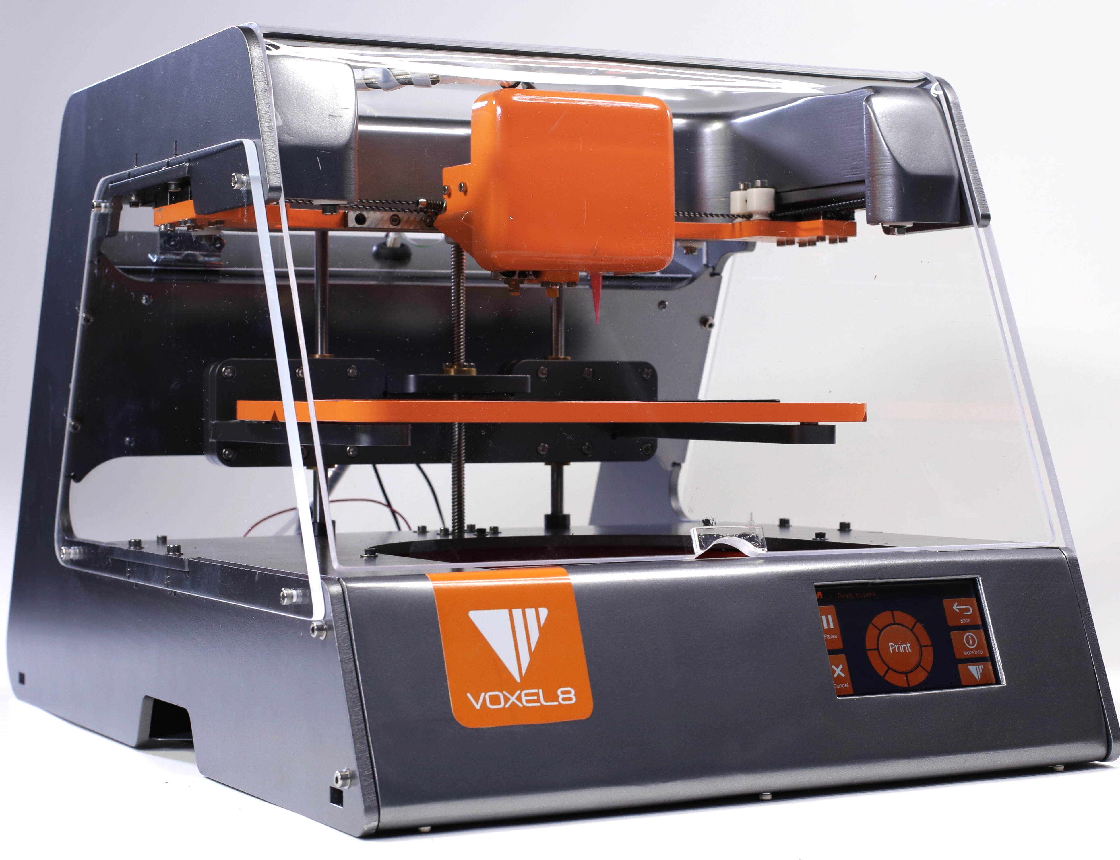
The Voxel8 system shown here combines plastic extrusion with silver-ink deposition and allows pauses for manual component insertion. The 2017 study describes limited capability for freestanding conductive structures in Z; recommended trace thicknesses below 500 µm concern that historical system.
Beyond deposition, the steps needed to obtain final electrical properties depend on the ink and substrate. Drying, thermal treatment, assembly and inspection must suit the materials and intended function.
Design data
Design data must describe geometry, conductive and insulating regions and component connections. Process preparation must translate that information into deposits and sequences compatible with the equipment.
A geometrically valid file alone does not establish that a circuit will meet its electrical requirements.
More data does not guarantee circuit quality or lower cost. Consistency, interpretation by the machine and verification of the result are the relevant requirements.
Final Thoughts
The examples in this feature show opportunities for prototyping and customisation. Material, energy, time and cost benefits must be assessed case by case, including treatment and assembly. Selection should begin with electrical performance requirements and manufacturing constraints.
THE 3D ADEPT WEEKLY NEWSLETTER
The industry moves fast. Stay ahead.
Every week, the latest additive manufacturing news, in-depth features and real-world applications, straight to your inbox. Plus, be the first to know when a new issue of 3D ADEPT Mag is out.
Free · One email a week · Unsubscribe anytime
Clicking loads our email provider’s sign-up form, including its analytics and Google’s anti-bot protection. You’re only subscribed if you complete the sign-up. Read our privacy policy.