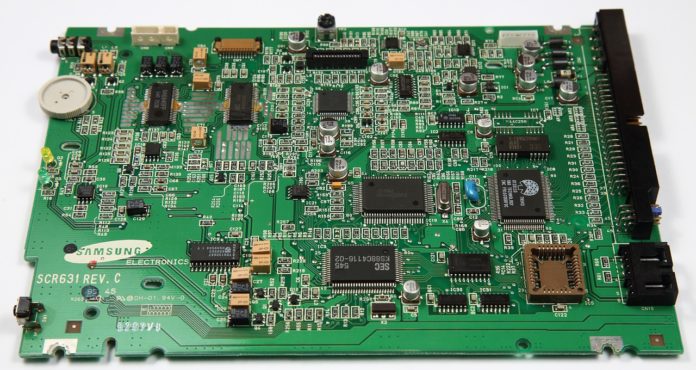
Today, Printed Circuit Boards PCBs are used in almost all devices. They have two main functions, affixing electronic components in designated locations and providing reliable electrical connections.
The entire process of organizing and fixing the PCB is known as PCB fabrication or PCB assembly. It is a procedure that transforms a circuit-board design into a physical structure.
To learn more about PCB fabrication, you should know the vital things.
What is PCB?
A printed Circuit Board or PCB is manufactured from layers of electric conductors, insulators, metal interconnects, and other elements. They are connected according to a design using copper tracks.
Today, PCBs are found in devices, including cell phones, televisions, computers, cars, and many other gadgets. They are created from various materials such as fiberglass and copper, with components soldered onto the board.
PCBs have numerous benefits that include safety from electrical hazards, ease of use, and mechanical support.
Even though they are primarily used in electronics, they can be found in other sectors. This is because they are the foundation of all electronic gadgets.
In addition, it is used in many fields such as industrial machinery, medical gadgets, lighting, and automotive industries, among others.
Moreover, various types of PCBs include single-layer PCB, Double-layer PCB, multi-layer PCB, and others.
Types of PCB
Single-layer PCB
Single-layer PCB is also known as Single-Sided PCB. It is simple and one of the most used Printed Circuit Boards. This is because it is easy to design and create.
With this type of PCB, only one side of the board is coated with a layer of conducting material. In most cases, copper is used since it is the best conducting material for PCB.
To protect the PCB against oxidation, a layer of solder mask is used and then silkscreen to mark the components on the board.
Being a Single-Layer PCB, only one side connects various electronic components such as an inductor, resistor, capacitor, and others. All these elements are soldered.
However, Single-Layer PCBs are used in low-cost applications such as radios, calculators, and printers.
Double-Layer PCBs
Double-Layer PCBs are also known as Double-Sided PCBs. It is a thin coat of covering material applied on both sides of the board.
The board is more flexible, lower cost, and has numerous benefits over the single-sided PCB. This type of PCB is mainly used in UPS systems, industrial controls, converters, HVAC applications, amplifiers, and phones.
Multi-layer PCB
A Multi-layer PCB is a more powerful PCB with more than two layers. It has at least three conductive layers of copper.
Since it is a complex board used in large electrical tasks in a shallow space, some of the significant applications that use this type of PCB include satellite systems, file servers, GPS technology, and medical equipment.
Others – apart from single-layer PCB, double-layer PCB, and Multi-layer PCBs, there are other types of PCBs. They include Flexible PCB, Rigid PCB, Flex-rigid PCB, and many others.
Manufacturing Process
PCB manufacturing is a complex process. This is because it has to factor in all the factors to ensure the finished product’s performance is at par. Even though there are various PCBs, the fabrication process is the same.
It may only differ after the first coat’s production. But due to modifications in structure, some PCBs may need more steps than others during manufacturing.
Below are the main steps of the PCB manufacturing process
1. Designing the PCB
The first step of PCB manufacture is the design. Here, there are various programs used by PCB designers to come up with a blueprint. The design logically represents multiple PCB components, electric circuitry, and traces.
After the design is complete, the finished design is sent to the PCB fabrication house for the PCB to be built. However, it has to undergo a second check to fulfill the acceptance required.
2. Printing the PCB design
The next major step is printing the PCB design. Unlike most plans such as architectural drawings, the PCB plans use a particular printer known as a plotter printer. Meanwhile, you can also print the design using a 3d printer.
The inner coats of the PCB are characterized in two ink colors, the black ink used for the circuits and copper traces, and the clear ink for the non-conductive areas of the board.
On the outer coat, the trend is reversed. The clear ink is for the copper traces, but the black ink is for areas where copper is removed.
3. Printing the copper for the interior layer
The third step is where the actual PCB starts to be manufactured. It begins with the basic form, where the PCB design is printed onto the laminate board. Then copper is pre-boarded on the board, both sides.
Then copper is etched to reveal the PCB design, and then the laminate board is covered with a photo-sensitive film known as a resist.
4. Layers Machining
Now the PCB is ready for layer machining and optical inspection, this process includes cnc machining and drilling holes in the board.
A technician places the layer on a punch machine during the layer machining. The machining aims to line up the layers of the PCB.
5. Automated Optical Inspection
After layer machining, PCB goes through another machine to ensure no imperfections. The process is essential because errors cannot be corrected when layers have been placed together.
After the PCB has passed the automated optical inspection and there are no errors, it can now be moved to the last steps of production. Without passing through this process, the boards may experience short circuits or fail to meet design specifications.
Summary
PCB fabrication is an intensive process that ensures the PCB comes out functional and durable. Fortunately, the advancement in PCB manufacturing has made it easier to manufacture compact and durable electrical gadgets.
Therefore, it is vital to understand the steps of PCB fabrication to unlock the true potential of PCBs. Happily, the above guide has explained all the things you need to know about PCB fabrication.


