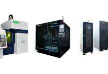
Provider of 3D printed electronics solutions, Optomec has released a new high performance semiconductor packaging solution for the rapidly growing mm-wave electronics market, in response to demands from its customers in the 5G, Autonomous Vehicle, Defense and Medical segments.
Millimeter-wave integrated circuit (IC) use is growing at 27% CAGR, but has been hampered in many applications because the traditional techniques used to connect the ICs to the circuits result in poor circuit performance in the form of low wireless range and/or high power consumption. Optomec’s 3D Printed Interconnect solution addresses this deficiency, preserving device performance with low loss connections.
Optomec customers have reported up to a 100% increase in transmitted signal power for each circuit connection in the millimeter range. This translates to longer point-to-point range for wireless data transmission, reduced energy consumption and, because lower-power ICs can operate at lower temperatures, increased IC life. The millimeter-wave frequency band comprises 30 to 300 GHz. Whereas today’s typical wireless network in the home or office operates at 5 GHz, next generation wireless mm-wave networks will operate at frequencies up to 53 GHz; automotive radar, defense applications and medical imaging sensors operate at even higher frequencies. The older methods of connecting ICs, such as the use of tiny gold wires, is less and less effective as the frequency increases, but the Aerosol Jet® method of printing the connection to ICs is much more efficient, with performance that nearly matches the etched copper traces of circuit boards.
“Our customers are reporting some very impressive performance improvements for mm-Wave interconnects”, said Bryan Germann, Optomec Product Manager. “Customers across many industries using millimeter wave frequency bands are seeing the benefits of printing interconnects in lieu of standard wire or ribbon bonds. The benefit of shorter, better impedance matched transitions lower losses for each die-to-die or die-to-board transition. This leads to improvements in overall device efficiency and performance.”
The Aerosol Jet® process works by jetting extremely fine droplets of nanoparticle conductive inks onto circuit boards and components from a distance of up to 10 mm away, yet it can produce conductive features as fine as 10 microns in width. Optomec’s new Aerosol Jet® HD2 printer with ultra-high printing resolution and integrated vision-based alignment has been optimized to support this new IC solution for full production applications. The HD2 supports standardized in-line automation for direct integration into existing packaging lines. Optomec further offers its customers pre-qualified printing recipes and application libraries for a total solution that is production ready.
Remember, you can post free of charge job opportunities in the AM Industry on 3D ADEPT Media or look for a job via our job board. Make sure to follow us on our social networks and subscribe to our weekly newsletter : Facebook, Twitter, LinkedIn & Instagram ! If you want to be featured in the next issue of our digital magazine or if you hear a story that needs to be heard, make sure to send it to contact@3dadept.com


