
")
As part of our ongoing efforts to spotlight solutions that support the adoption of additive manufacturing (AM) in electric vehicle (EV) applications, we stumbled upon the “Dauerpower” project — a collaboration between the Fraunhofer Institute for Reliability and Microintegration (IZM), Bosch, and Porsche. Together, they developed a high-performance power inverter designed to meet the demanding requirements of next-generation EVs. Delivering peak outputs of up to 720 kilowatts, the inverter leverages silicon carbide (SiC) semiconductor technology alongside 3D-printed cooling components. At its core, the use of SiC transistors enables long-term load stability while significantly reducing energy losses. This initiative, in conjunction with recent coverage from 3D ADEPT Media, triggered several questions on silicon carbide parts manufacturing — an area that extends far beyond semiconductors and warrants closer examination to fully grasp its industrial potential.
Described as the third hardest material in the world, silicon carbide is not only in high demand—it’s also complex, especially for those unfamiliar with it. This compound of silicon (Si) and carbon (C) exists in multiple crystalline forms, though not all are suitable for additive manufacturing (AM). With a key focus on silicon carbide (SiC) ceramics, this clarification is what Johannes Homa, CEO and founder of ceramic 3D printing company Lithoz, emphasizes from the outset:

“Silicon carbide (SiC) ceramics come in several forms depending on how they are made. I have summarized here the most common types:
- SSiC – Sintered Silicon Carbide: This is SiC in its purest ceramic form. It is a very fine SiC powder pressed together and baked at extremely high temperature until the particles fuse into a solid part. This makes it exceptionally strong, hard (almost as hard as diamond), and chemically inert, with a density comparable to other ceramics. Importantly, SSiC stays robust even at very high temperatures; it barely loses strength up to about 1,600 °C. In short, SSiC is a high-performance pure ceramic, ideal for demanding roles that need maximum strength and heat resistance.
- SiSiC – Silicon-Infiltrated Silicon Carbide: In this type, silicon carbide is “glued” together by a reaction with molten silicon metal. The manufacturing is a two-step approach: first a SiC part with coarse powders is formed (often mixing in some carbon), which is then infiltrated with liquid silicon. The silicon is soaked in when melted during the heat up and reacts then with carbon (from the binder and also added) to create more SiC, bonding everything. The result is a composite: mostly SiC but with some leftover metallic silicon filling the gaps (usually around 10–15% by volume). Hence it is also sometimes referred to as reaction-bonded SiC (also called RB-SiC). It is easier to produce in complex shapes, because it does not shrink and can he sintered at lower temperatures. Due to the silicon in the material, it does not have the same strength and is not as heat-resistant as the SSiC. The leftover silicon is a bit of a weak link. It limits the maximum use temperature (the free silicon melts at about 1414 °C, so these parts are generally safe only to ~1350 °C before they soften). Also, the extra silicon can slightly lower the overall hardness and purity of the ceramic. Still, SiSiC is popular for things like furnace components and kiln furniture, where making large, complex parts with good thermal shock resistance outweighs the need for ultra-high strength.”
That said, given its growing use in semiconductor devices within various industries, SiC is seen as an important industrial ceramic material that can be used for structural purposes. Sarah Diener, Head of Additive Manufacturing at KYOCERA Fineceramics Precision GmbH – a ceramic 3D printing service bureau -, explains: “SiSiC, known for its high stiffness and low thermal expansion coefficient, is often used for structural components. For structural components, the weight is important. By design optimization, lightweight structures can be thought of, which result in complex part geometries. Those geometries can often only be made by AM.”
AM approaches to silicon carbide parts
First, SSiC – Sintered Silicon Carbide
For the record, through conventional manufacturing approaches, Sintered Silicon Carbide (SiC) is often processed by Cold Isostatic Pressing (CIP), injection molding, or pressureless sintering.
SiC 3D printing can be challenging, mostly due to the material’s high melting point and the need for specialized equipment and techniques. Due to these sintering constraints, it’s fair to say that SSiC (Sintered Silicon Carbide) is not yet common in industrial AM production.

“The properties of silicon carbide are especially relevant to developments in the industry today, in terms of hardness, its durability in extreme conditions, its semiconductive properties, its toughness and its very low thermal expansion coefficient.
It is especially interesting for additive manufacturing because the traditional method of manufacturing involves milling the material which is both slow and, because of the materials’ hardness, very tough on the tooling used. With 3D printing many forms can be realised in a very quick manner with much less wear on the tooling,” Eric Geboers, founder of CONCR3DE adds.
Although they would need various post-3D printing processes to achieve the desired part, the most commonly used AM processes that could be explored to process this material include: Lithography-based Ceramic Manufacturing (LCM), Binder Jetting, Direct Ink Writing (DIW), and Stereolithography (SLA). However, most applications remain at the research stage for these technologies.
Emphasizing the challenges at the post-processing stage, CONCR3DE’s founder said it requires specialized knowledge and kilns. “If you already process silicon carbide taking up 3D printing will be easy as it is known technology, if you are a new service provider looking to produce silicon carbide parts there will be a more steep learning curve. This can be solved by working with known kiln providers who possess knowhow on post processing silicon carbide, but there are some peculiarities to the material that are different than dealing with metals or plastics,” it adds.
“Due to its unique properties and the fact that it requires exceptionally high-temperature sintering, SiC is challenging to thermally process using any technology. Traditional processes have, of course, much more experience with this material, but the thermal challenges are basically the same.
The sintering temperature for silicon carbide (SiC) is typically in the range of 2,200°C. SSiC (sintered silicon carbide) is SiC in its purest ceramic form. As mentioned, this makes functional parts made from silicon carbide extremely durable; they barely lose strength at temperatures of up to 1,600 °C. However, apart from the extremely high energy consumption of thermal processing, these requirements are difficult to meet. A viable solution for easier treatment has been found: SiSiC (silicon-infiltrated silicon carbide). In short, silicon carbide is ‘glued’ together by reacting with molten silicon metal. This is a two-step process: first, a coarse powder SiC part is formed, which is then soaked in liquid silicon. During the heating process, silicon reacts with carbon. The result is a composite material called SiSiC. It does not shrink and can be sintered at lower temperatures. However, the presence of silicon means that SiSiC is not as strong or heat-resistant as SiC; these parts are generally only safe up to ~1350 °C before they soften,” Homa confirms.
Speaking of lithography-based printing processes, he explained that they are faced with the challenge of the material’s dark color that absorbs the light necessary to expose the layers.
Second, SiSiC – Silicon-Infiltrated Silicon Carbide
Most AM SiC parts today are SiSiC due to easier processing.
Homa told 3D ADEPT Media there is a growing interest in slurry-based technologies and their ability to process SiSiC. These technologies include LIS (Laser-Induced Slip casting) and LSD-Print (Layerwise Slurry Deposition), they are developed at BAM (Bundesanstalt für Materialforschung und -prüfung) and commercialized by Lithoz,
“These two technologies are still in the early stages. Nevertheless, the current trajectory is promising. Research, development, and investment are accelerating, and once the supply of the material, the reliability of the process, and the post-processing chains are more established, we can expect to see rapid growth in the industrial-scale adoption of these technologies,” Homa notes.
However, all experts contributing to this dossier mention binder jetting as the AM process that has successfully achieved SiSiC parts.

“SiSiC is not a classical ceramic”, Sarah Diener said. “It is not sintered but infiltrated with liquid silicon. The liquid silicon reacts with carbon in the printed preform and forms secondary SiC. The not reacted silicon fills the pores of the material. Unlike in polymer or metal AM, in ceramic AM, a heat treatment, classically a sintering step, is needed to create the final ceramic part. The AM method is basically used for shaping the part. [Binder Jetting] is the perfect AM process for that material, as the used particle size is comparably high and thus the flowability of the material is good for the powder deposition. Due to the infiltration process, instead of a classical sintering step the porosity that is left in the part after printing is not a drawback but even needed. Moreover, many SiSiC are large ceramic parts and thus binder jetting is also more suited than, for example, material jetting. Other methods like VAT are difficult to realize due to the high absorption of the SiC.”
Geboers completes these statements by highlighting a key performance indicator of the manufacturing process with binder jetting:
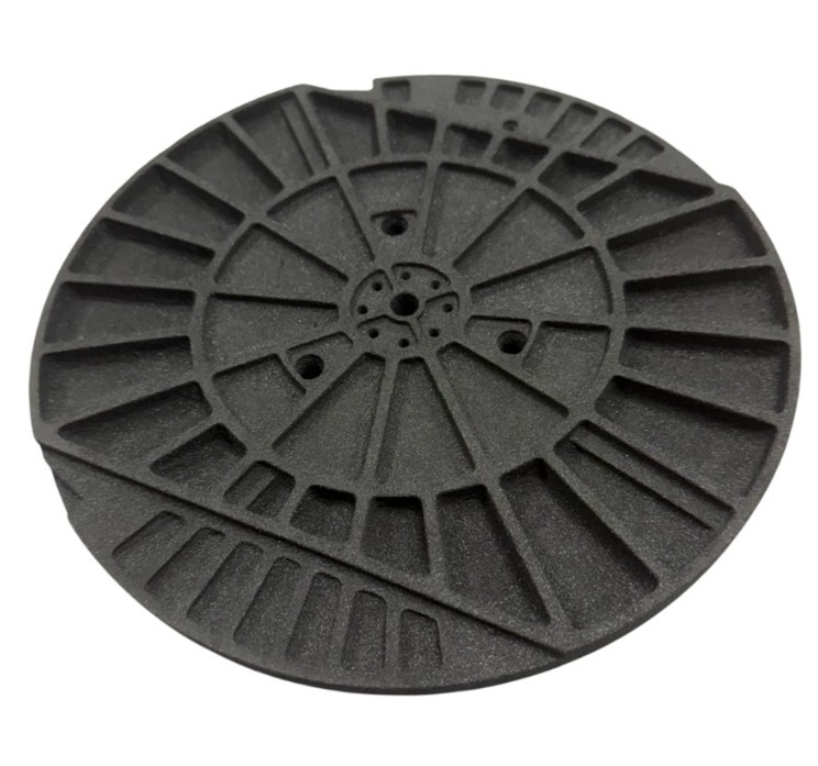
“There is a good technology match between SiSiC (silicon infiltrated silicon carbide) and binder jetting. Binder jetting silicon carbide body typically results in a porous green body, which is highly suitable for silicon infiltration, which is already a known process in the ceramic industry. And, because you are infiltrating with silicon rather than sintering, there is absolutely minimal shrinkage in the post processing stages. This, in turn, allows the user to make very large forms with high tolerances.
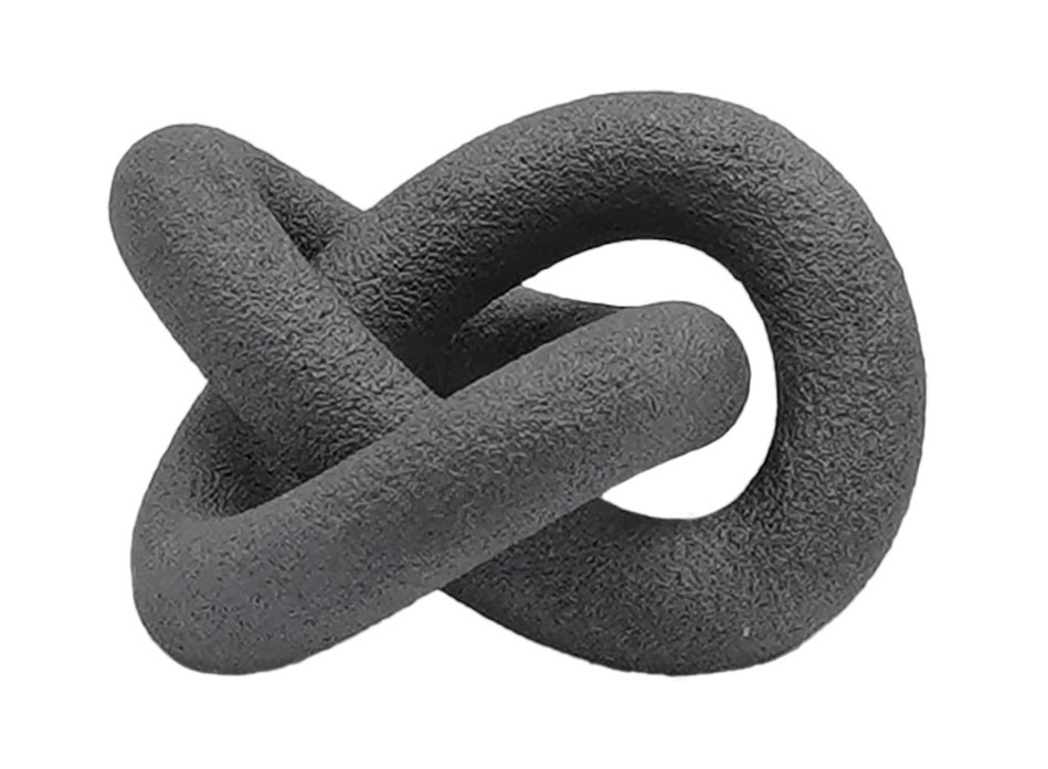
A typical important performance indicator of a SiSiC part is its density which is influenced both by how the green body is made in the printer and how the post processing is done. Typically, a higher final density requires a more complex printing and post-processing strategy. A fairly straightforward SiSiC with a density of 2,8 g/cm3 can be achieved purely by printing an aqueous binder and then debinding and infiltrating. Higher densities can be achieved via the addition of carbon in the powder and the use of particle-filled inks, which greatly increase the green density. Carbon can also be added to the green body by dipping parts in resin and pyrolyzing them – this process, however, involves rather nasty chemicals, and we at CONCR3DE have a strong belief in sustainability. Our preferred method that we work out with customers is therefore the use of particle-filled inks, which allow the density to be above 3,05 g/cm3 – making them useful for even the semiconductor industry.”
CONCR3DE have already produced small parts (down to 40µm) and very large parts (up to 2 meters in length). These parts are usually post processed with silicon infiltration but they can also be processed via SPS (spark plasma sintering) for high resolution, high-density small parts.
Key applications of 3D printed SiSiC – Silicon-Infiltrated Silicon Carbide parts
3D-printed SiSiC (silicon-infiltrated silicon carbide) parts are already being used in industry, and the process is scalable thanks to the availability of large-format printers originally developed for sand printing. All three experts identify the semiconductor industry as the main beneficiary of this material. While not directly tied to SiSiC, Homa recently highlighted it as a key enabler in semiconductor applications in this conversation with 3D ADEPT Media.
Beyond the semiconductor field, Homa explains that components that require high thermal conductivity, strength (even at elevated temperatures), light weight, and wear resistance could benefit from this material.
Applications outside the semiconductor field, then include nonlinear conductors, atomic energy applications, and space technology.
“We’re seeing growing interest from the defense and aerospace sectors, where SiC-based components are used in applications such as gun silencers, optics, rocket nose cones, heat shields, and body armor. Another high-potential area is the nuclear industry, and even the automotive sector is exploring its use—for example, in high-performance brake discs,” Geboers concludes.
Concluding thoughts
SSiC still holds promise for its superior purity and mechanical strength, but its path to additive manufacturing remains hindered by sintering limitations.
However, as SiSiC gains traction in additive manufacturing, its growing adoption in industries like defense, semiconductors, and optics confirms both its technical relevance and scalability. Yet, only binder jetting is currently leading the way. Slurry-based AM technologies—like those explored by Lithoz—could open new pathways for processing even more complex or performance-demanding parts. As materials and machine capabilities continue to evolve, we’ll be keeping a close eye on how these technologies and more could further process silicon carbide and integrate into the expanding world of ceramic 3D printing.
Editor’s notes
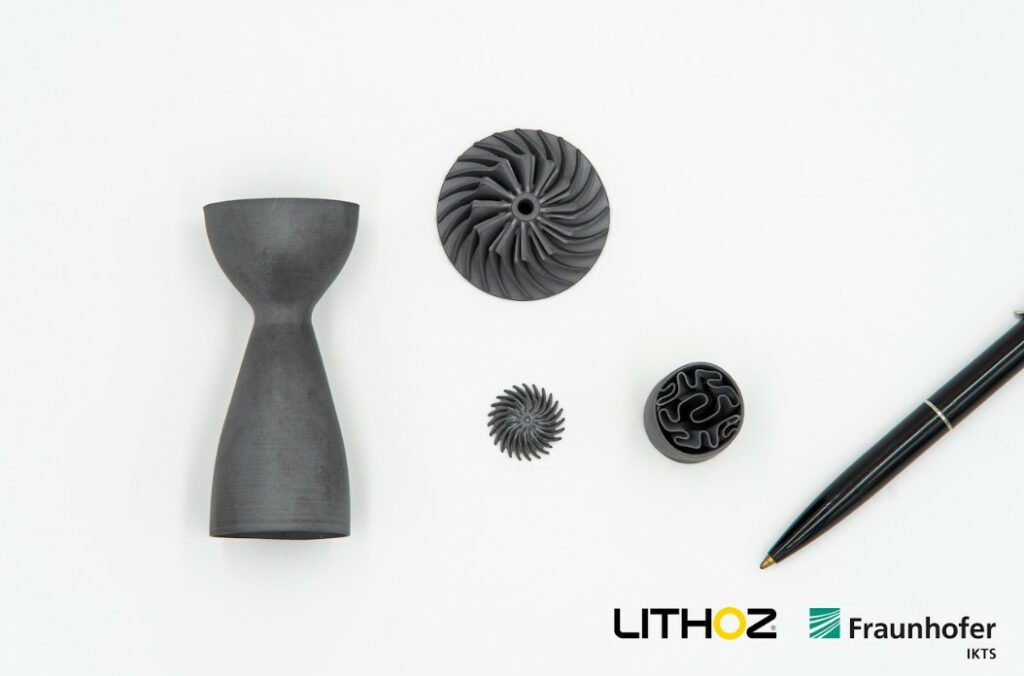
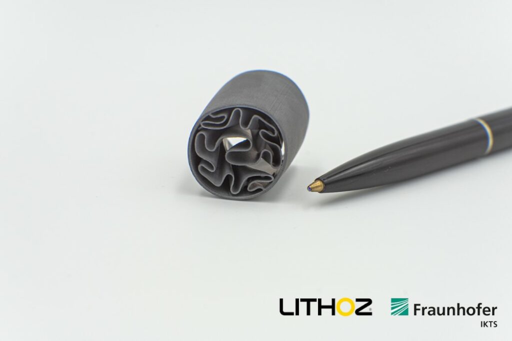
Known for its lithography-based printing processes, Lithoz is a global provider of high-performance ceramic materials and 3D printers, committed to breaking the boundaries of ceramic production. The company was invited to this dossier due to the potential its LIS and LSD-print technologies hold for SSiC. Although they are still in stealth mode with these technologies, the company is currently looking for partners who require SSiC.
CONCR3DE first came onto our radar four years ago for its work in the construction industry. Today, the company is expanding its installed base while qualifying advanced technical ceramics, including alumina, zirconia, and silicon carbide. By fine-tuning raw materials, binder chemistry, and printing parameters, CONCR3DE is able to produce both small, intricate components and large, complex parts—with material properties tailored to specific customer applications.
KYOCERA Fineceramics Europe GmbH, a subsidiary of KYOCERA Europe GmbH, a supplier of advanced ceramic components for the technology industry, recently established a process for the additive manufacturing of components made of silicon carbide (SiSiC) at its Selb location in Germany. Sarah Diener has been working on the AM of SiSiC for more than 8 years and is the team leader of the R&D group on AM at KYOCERA Fineceramics Europe in Selb.


")