

The semiconductor industry always seemed to me to be a distant industry where AM would not have a major role to play, until the recent Formnext edition, where I saw several interesting applications enabled by this technology. The more I dive into this topic, the more I realize that these are two sectors that can help each other.
For those new to semiconductors, it’s essential to note that this industry encompasses everything related to the design and fabrication of semiconductors and semiconductor devices, including transistors and integrated circuits.
“When we talk about the semiconductor industry, we’re referring to the electronic chips that are everywhere around us, from phones, tablets, data centers and accelerators to cars, airplanes and satellites. The semiconductor capital equipment (SCE) industry makes the equipment utilized to make those chips. As far as manufacturing is concerned, one important point we need to clarify is that there is often confusion between printed electronics and AM applications in the semiconductor industry. These are two different topics, and they should be discussed separately,” Dr. Ahmed El Desouky, Director of Additive Manufacturing at Veeco, clarifies from the outset.
While this sector is the driving force behind the wider electronics industry, it is the supply-demand imbalance that governs the year-on-year dynamics. Interestingly, the challenges that arise across this supply chain somehow led to the opportunity to use AM.
This dossier aims to help industrials understand:
- The supply chain issue that led to the exploration of AM as a production candidate in the semiconductor industry (Moore’s law)
- The use of AM in the semiconductor industry
- Challenges & future outlooks
While we aim to highlight a wide range of applications enabled by AM, a key focus will remain to understand the challenges and use cases specific to semiconductor capital equipment manufacturers.
Moore’s law
According to Dr. El Desouky, Moore’s law best illustrates the opportunity Semiconductor Capital Equipment (SCE) manufacturers have seen in exploring the use of AM.

“Sixty years ago, Moore[1] observed that the number of components per integrated circuit will double every 2 years, and this law has held since then”, Dr. El Desouky explains.
Several decades later, one observes that as time goes by, devices produced by OEMs across the world are more and more complex, and so is the complexity of microchips that power them.
Such complexity has triggered a cycle where semiconductor companies face great pressure to deliver higher performance and reliability in their equipment. To do so, SCE manufacturers need enhanced manufacturing lines that can meet these high-performance requirements. Unexpected supply chain issues can slow down production cycles and result in long lead times of up to 12 months before the completion of an equipment.
“Semiconductor Capital Equipment manufacturers like Veeco play a critical role in upholding Moore’s Law, but doing so involves significant technological challenges. This also presents an opportunity for adopting new technologies such as Additive Manufacturing. The need to constantly and quickly develop new materials, processes, and architectures aligns perfectly with the design freedom and innovation that AM brings to the table,” The Director of AM points out.
The use of AM in the semiconductor industry
It is now clear that SCE manufacturers turn to AM to produce parts for their existing machines or to manufacture highly sophisticated components.
At Formnext 2024, and through our coverage of this vertical industry, we identified Laser powder bed fusion, Directed Energy Deposition (DED), Metal Binder Jetting (MBJ), Bound Metal Deposition (BMD), SLA, electrohydrodynamic (EHD) inkjet printing, and lithography-based ceramic manufacturing as AM processes that could be explored in semiconductor applications.
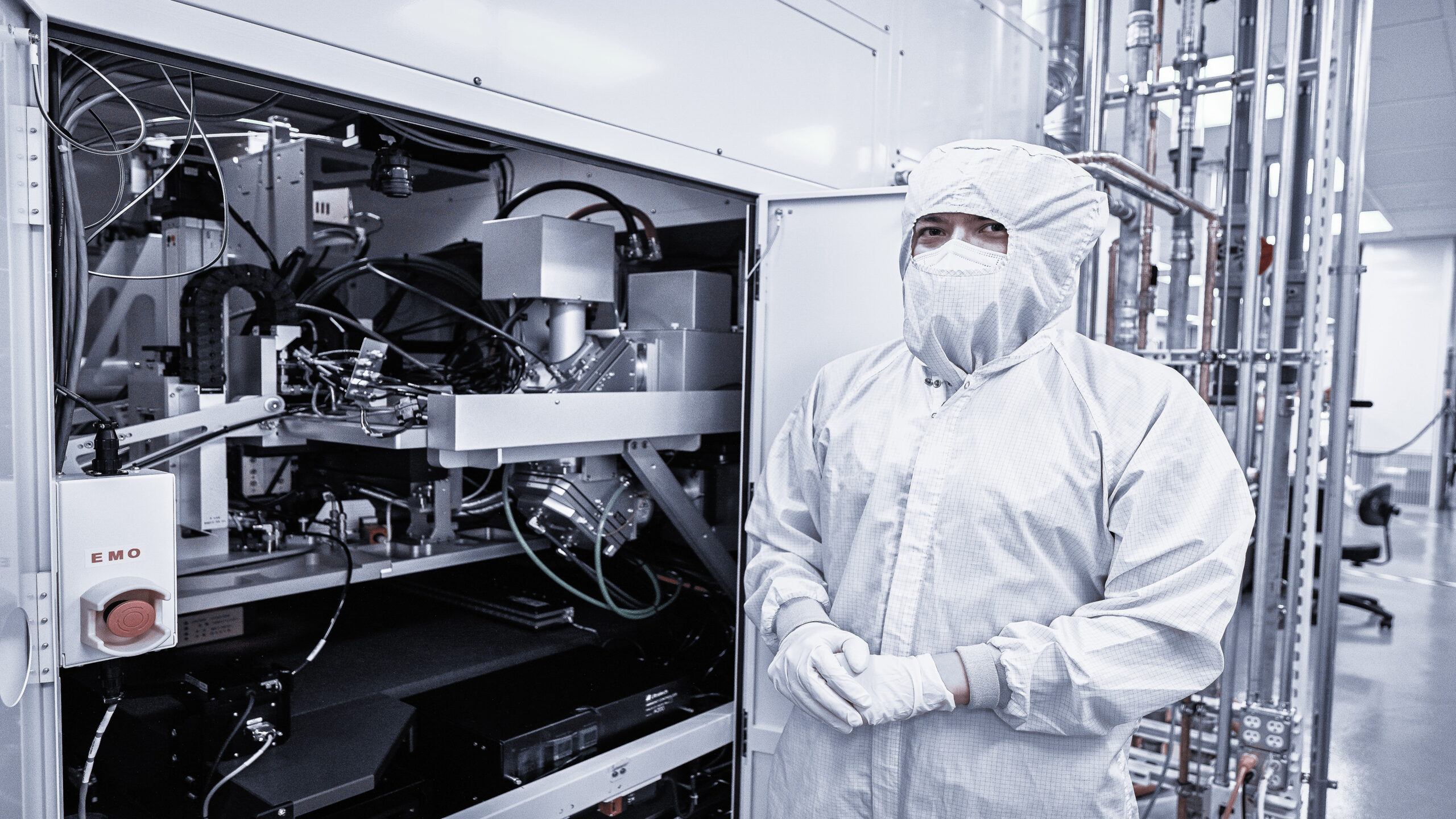
For Dr. El Desouky, “Among all these technologies, the more mature one remains Laser powder bed fusion. That’s the AM process we are using the most right now as last year Veeco acquired the NXG XII 600 system from Nikon SLM Solutions to achieve our production objectives,” he adds.

“There are dozens and dozens of applications that use semiconductors but the way they affect the supply chain is mostly in communication networks, network infrastructures, and end-user devices. That being said, semiconductor manufacturing is a highly intricate process that relies on various types of capital equipment to perform many different tasks,” AM Engineer Eilis Taylor said to introduce the applications enabled by AM. These tasks may include gas mixing, deposition, masking and slicing.
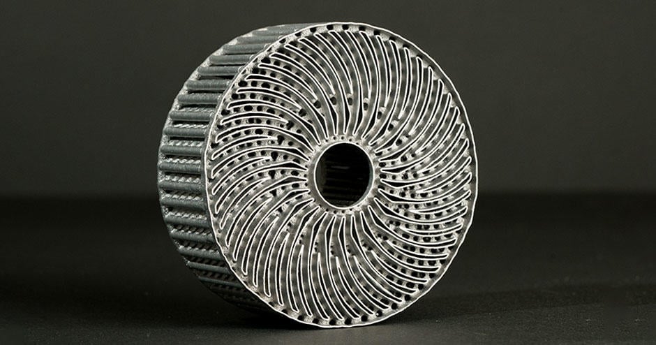
As we have already seen through lattice structures within heat exchangers, AM remains an ideal production candidate for the creation of intricate structures. So far, three categories of applications are gaining momentum in this field: optimization of structural parts, thermal management and fluid flow optimization.
“At Veeco, some of the primary applications where AM plays a key role include gas injectors for manifolds and water-cooling heat exchangers,” Taylor notes.
If we only look at heat exchangers whose application has been widely covered through 3D ADEPT Media, one will realize that traditional manufacturing techniques used for their production are often inefficient due to bulky designs of parts. Thanks to the fabrication of lattice structures and intricate channels, AM provides an opportunity to enhance heat exchangers of SCE.
The improved thermal management is often seen in parts like wafer tables where AM can help enhance accuracy by 1–2 nm while increasing machine speed and uptime.
“Since we are 3D printing machine parts, we can explore a lot of material combinations in this industry (metal, plastic, ceramic…)”, Dr. El Desouky starts.
“The reality is that most of the process combinations that exist were first designed for other industries. Those industries that first adopted AM develop the materials that are specific to their applications, and that’s what we need to do in the semiconductor industry where AM is still in its infancy,” Taylor continues.
“There is room for expansion in many areas, in refractory metals and ceramics. We don’t have to use the same alloys that we’ve always used in casting and machining. We could look for alloy designs that could meet the specific needs of certain applications in semiconductors,” Dr. El Desouky adds.
 Challenges & future outlooks
The conversation with Veeco’s experts highlights material selection and qualification as a major challenge for SCE manufacturers. AM materials that could meet the stringent performance requirements of semiconductor devices could be challenging to identify as they should be able to deliver electrical, thermal, and mechanical properties – all of which are crucial to unlocking the potential of AM in semiconductors.
Although the semiconductor industry does not suffer from the “regulation burden” of industries like aerospace, manufacturers of this industry must still address the “repeatability” challenge that is inherent to the use of AM and related processes.
We didn’t discuss this point, but I believe the ‘repeatability’ constraint could pose challenges when scaling up AM in this vertical—particularly when trying to maintain consistent device performance.
Given that we are still in the early stages of adopting AM in this vertical, it’s not surprising that the cost per unit for certain components might remain relatively high compared to traditional manufacturing processes. However, as with many applications in other industries, the use of AM in this vertical should always be “product-driven.”
Lastly, the lines above may emphasize how AM benefits the semiconductor industry, but the challenges that remain to be addressed will urge AM technology providers to collaborate with SCE manufacturers to develop solutions that are specific to semiconductor applications.
Editor’s notes
To discuss this topic, we invited Dr. Ahmed El Desouky, and Eilis Taylor from Veeco Instruments. Their comments have been edited to maintain clarity and brevity. All other images: courtesy of Veeco.
Veeco is a global designer and manufacturer of semiconductor process equipment for wet and laser processing, lithography, ALD, CVD, MBE, PVD, and more. The company has been exploring the applications possible with AM for a few years now, but its recent acquisition of NXG XII 600 positions the company as one to watch in the semiconductor industry.
[1] The law is named after Gordon Moore, co-founder of Fairchild Semiconductor and Intel and a former CEO of Intel.


