


A feature first published in the July/August 2023 issue of 3D ADEPT Mag, co-written by Andrew Miller and Kety Sindze. The outlook and author biographies refer to that period.
Among the technologies that could broaden additive manufacturing applications, nanotechnology can be difficult to place. The two fields can open opportunities in healthcare, electronics and other sectors. Understanding those prospects requires a distinction between making very fine structures and using nanomaterials in larger parts.
What does working at the nanoscale mean?
Nanotechnology is not limited to tiny robots or to 3D printing small parts. It draws on physics, chemistry, biology and different engineering disciplines to study and use matter at a very small scale.
A nanometre is one billionth of a metre, or one thousandth of a micrometre. The National Nanotechnology Initiative generally places the field at approximately 1–100 nanometres. A nanoparticle is not simply an isolated atom: it can contain many atoms. At this scale, surface-to-volume ratio and other size-dependent effects can change material behaviour.
Making fine structures: distinguishing the processes
One connection involves using fabrication techniques to produce structures with micro- or nanoscale details. Resolution needs careful description: layer thickness, lateral feature size and overall object dimensions are different measurements. One value therefore cannot represent every additive manufacturing system.
Two-photon polymerization can create resin structures with submicrometre details. Dip-Pen nanolithography uses a tip to deposit molecules on a surface. Atomic layer deposition forms thin films through successive surface reactions. These processes have different purposes and capabilities; they should not all be described as equivalent 3D printers.
Electron beam melting of a metal powder bed is a different process again and should not be equated with nanoscale fabrication. For very fine structures, precision, achievable size, material and manufacturing throughput need to be considered together before assessing industrial use.
Incorporating nanomaterials into printed parts
The second connection concerns material formulation. Nanoparticles or nanotubes can be introduced into a matrix, such as a polymer or ceramic, to form a nanocomposite. The final part may be several centimetres across: nanoscale constituents do not mean that the part itself was printed at that scale.
Filled-resin development illustrates this approach. Mechnano works on carbon nanotube functionalization and dispersion, with Tethon3D among its formulation partners. Target properties may concern electrical, thermal or mechanical behaviour. They depend on the formulation and testing and do not necessarily all improve together.
Composite materials can be developed for filament extrusion, laser sintering or photopolymerization, subject to compatibility with each process. Filler dispersion, agglomeration, viscosity and response to light or heat influence fabrication. Adding a filler therefore does not automatically make a material printable or, by itself, resolve limitations in available feedstocks.
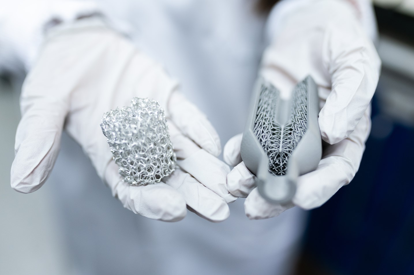
Assessing risks to people and the environment
Safety needs to accompany material development. As NIOSH explains, effects and exposures need assessment for the nanomaterials involved. Composition, shape, dose and exposure routes matter. Small size alone is insufficient to conclude that a material is harmless or, conversely, that it presents the same risk as another material.
Feedstock preparation, printing, finishing and end of life can create different exposure situations. A filler embedded in a part and a free powder are not handled under the same conditions. Assessments, preventive measures and applicable requirements need to be defined for the activity, without extrapolating the safety of one consumer product to all nanomaterials.
Biomedical and electronic prospects
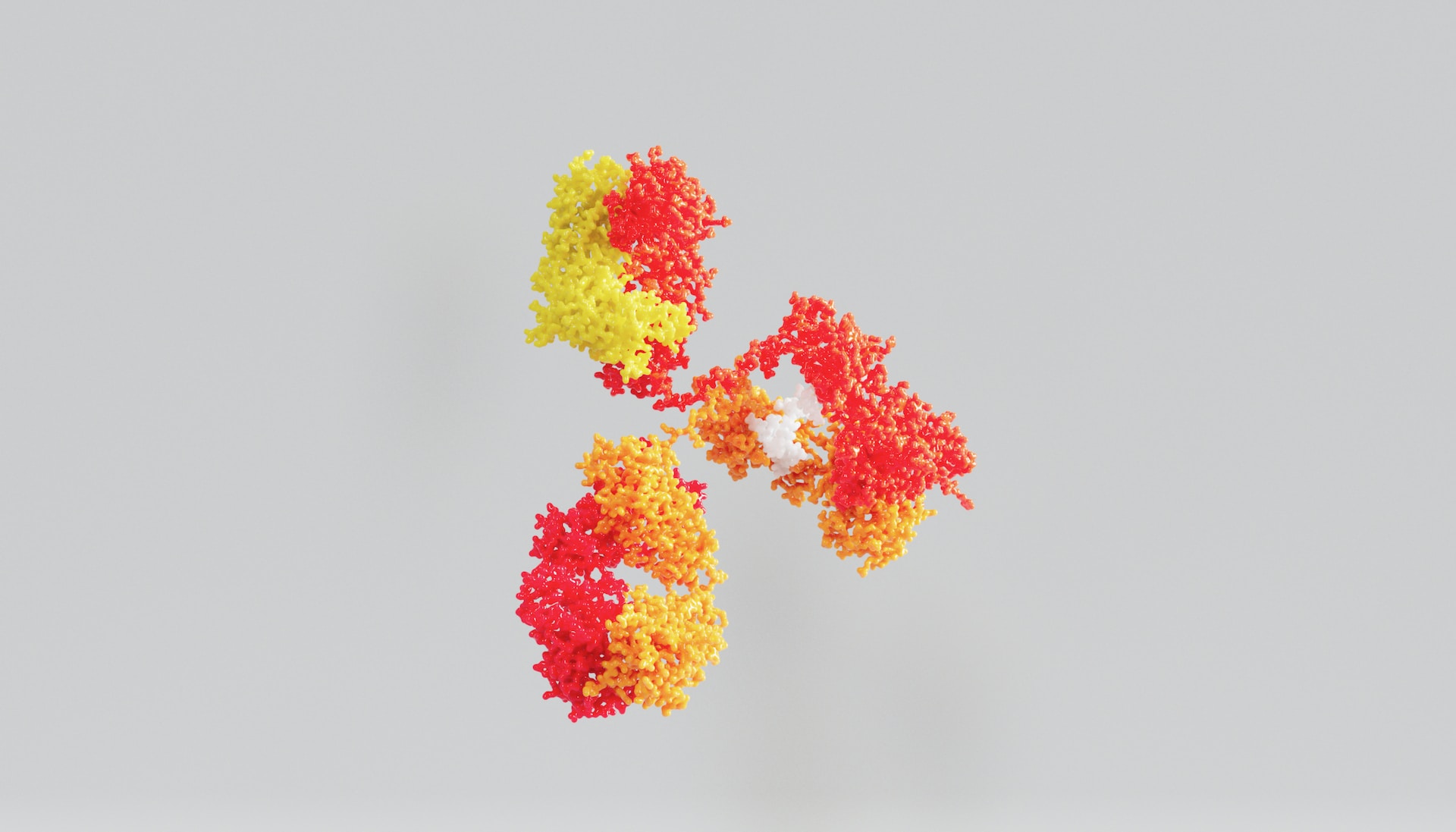
Biomedicine and electronics offer opportunities to use nanocomposite properties. A formulation may target particular conductivity, mechanical behaviour or interaction with a biological environment. Selection depends on the functional need; improvement measured in a laboratory still needs verification in the part and its operating conditions.
Research on polymethyl methacrylate (PMMA) bone cements investigates additions such as hydroxyapatite or carbon nanotubes to modify mechanical behaviour. These are material research avenues. They do not, by themselves, demonstrate improved clinical joint fixation or validate a 3D-printed cement for that use.
Photopolymer resins, thermoplastics and metallic materials each present formulation and processing constraints. For powder bed fusion or directed energy deposition, effects of the thermal cycle are among the factors to investigate. It would be premature to rank these families by a universal ease of nanotechnology adoption.
Bringing the fields together remains promising for tailoring properties and making new geometries. Industrial value depends on reproducible results, part qualification, risk control and the cost of the complete process chain. It does not guarantee perfect surfaces or identical performance across applications.
About the authors
This feature was co-written by Andrew Miller and Kety Sindze of 3D ADEPT Media. Trained as a mechanical engineer, Andrew Miller described his intention to devote his career to additive manufacturing and nanotechnology. A co-author of two publications on metal additively manufactured heat exchangers, he reported experience with fracture mechanics of rocket-engine components while working as an aerospace engineer at Blue Origin.
In his 2023 biography, he explained that this interest had led him to deepen his materials-science knowledge in the Johns Hopkins Engineering for Professionals graduate programme. He cited lessons from Professor John Slotwinski, identified in the contribution as Chair of the ASTM Executive Committee on AM technologies, and his ambition to develop new applications combining the two fields.
First published in the July/August 2023 issue of 3D ADEPT Mag.
THE 3D ADEPT WEEKLY NEWSLETTER
The industry moves fast. Stay ahead.
Every week, the latest additive manufacturing news, in-depth features and real-world applications, straight to your inbox. Plus, be the first to know when a new issue of 3D ADEPT Mag is out.
Free · One email a week · Unsubscribe anytime
Clicking loads our email provider’s sign-up form, including its analytics and Google’s anti-bot protection. You’re only subscribed if you complete the sign-up. Read our privacy policy.