

Feature first published in the March/April 2021 issue of 3D ADEPT Mag. Interviews and examples describe solutions presented at that time; functions and performance still need verification for each installation.
The Internet of Things (IoT) connects devices and software to use operational data. In additive manufacturing it can help monitor machines and parts. Conversely, additive technologies can help manufacture components for connected devices. This feature examines both relationships.
Connected devices can measure, send and receive data over wired or wireless networks, directly or through gateways. Automation depends on the application: a network connection does not eliminate configuration, maintenance or supervision.
Home automation is a familiar application: lighting, heating, audiovisual equipment or security systems can be controlled and monitored remotely. It is neither the sole origin nor the definition of IoT; industrial uses face different constraints.
Over time, with the digital transformation of manufacturing, manufacturers have outlined this system of interrelated points as a core component of industrial transformation efforts hence the term Industrial IoT (IIoT).
Gravity Pull Systems, Nano Dimension and Twikit approach this relationship from different businesses. Their interviews distinguish data-collection and processing functions integrated into production from connected devices whose components may be made additively.
Martijn Joris, founder & CEO at Twikit states from the outset : “The relation between IoT and AM goes in both directions. IoT can be used to industrialize AM processes, just like AM can be used to prototype and produce IoT devices.”
“We believe that IoT is rather a module than an application. Depending on the utility of the IoT device, its purpose is mainly ‘data collection’ in our case. Therefore, we use IoT more intelligently than a simple hardware ‘add-on’. Data collected from a single device is usually part of a larger transaction where multiple devices and potentially additional business logic are needed to complete a transaction. We implement that consistency right in the edge”, outlines Huba Horompoly, Founder & Managing Partner at Gravity Pull Systems, Inc..
“For Nano Dimension, it’s an application. For us, IoT is something that needs to communicate. The recent advancements of additive manufacturing are currently enhancing product development processes and the way engineers design for several vertical markets. When we look at what we call “Additively Manufactured Electronics” (AME), there is a big potential for IoT devices”, states Valentin Storz, VP Marketing & General Manager EMEA at Nano Dimension.
We first examine IoT as part of a production environment, then additive manufacturing as a way to make components for IoT devices.
IoT in additive production

An IoT solution can combine sensors, connectivity, software, interfaces and data processing. The elements required depend on equipment, the information sought and the decisions that information is intended to support.
These systems acquire, transmit and interpret data using rules or models. Reliability depends on sensors, networks, data quality and validation of processing; it is not an automatic property of IoT.
Shop-floor monitoring and control are among the uses associated with Industry 4.0. Machine information can support planning, equipment monitoring and production records. Gravity Pull Systems presents Synoptik as a software platform linking order entry, planning, production and post-processing. These are the company’s stated functions; the scope depends on integration at each site.
“Our IoT solution does not require specific tasks”, Horompoly explains. “There are several in-situ process monitoring applications available on the market. We excel in integrating the information generated by those solutions with our production logistics IoT apps, so we get a holistic picture immediately with analysed co-relations instead of a set of ‘raw data’ only. We do not simply collect raw data with our IoT apps and self-developed sensors but put them into the right context; this enables Synoptik to give recommendations on possible actions, to react on IoT generated events in real time. Since our software links every event with costs, we recommend the optimal course of next actions not merely on the logistics level, but also based on financial insights that our optimizer detects based on pre-defined cost accounting principles.”

Solukon presented its Digital Factory Tool in March 2021 for automated depowdering. The supplier describes production monitoring, maintenance, automation integration and quality-documentation functions. Its systems had been offered with an OPC UA interface since 2017. OPC UA stands for Open Platform Communications Unified Architecture; it provides a framework for exchanging data and information models.
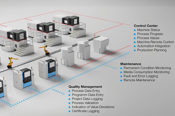
The feature describes a Solukon SFM-AT800 at Fraunhofer IWU in Dresden within a modular robotic cell, alongside geometry inspection, support removal and handling operations. OPC UA provides a communication framework; working interoperability also depends on the interfaces and information models implemented by each station.
Related reading: Solukon’s digital functions for depowdering.
A scenario where IoT solutions are well integrated in a smart manufacturing environment is ideal for any industry, but its share of challenges often slows down its proper integration. These challenges include for instance:
- Vulnerable components. Given the interconnection with a number of security disciplines, it is important to look at the convergence between IT security, OT security and physical safety and the shift from closed to connected cyber-physical systems.
- Supply chain complexity. This is a “pain point” for manufacturers of products who often rely on third parties’ components for certain productions. This might result in an extremely complex supply chain with a large number of people and organisations involved that need to be managed. According to the team of security experts at Secure Thingz Ltd., not being able to track every component to its source means not being able to ensure product security, which is only as secure as its weakest link.
- Another challenge comes with the fact that industries need to secure product lifecycle – “device security should be a subject of consideration through the product’s entire lifecycle, even end-of-life/end-of-support of the machine.”
Security needs to cover devices, users and the full support lifecycle. NIST guidance published in 2020 includes device identification and configuration, data protection, interface access control, updates and visibility of cybersecurity state. Remote access should be limited to operational needs.
When asked how their solution addresses this security issue as part of an AM production environment, the Managing Partner at Gravity Pull Systems, Inc. declares:
“We developed a solution where any machine (or manually) generated data is validated by a private/public key pair, the validator being installed on a NFC Chip. Before being saved in a database or a blockchain, all data go through this process. We ensure end-to-end data transparency by the application of this infrastructure.”
A cryptographic signature can help verify data origin and integrity. It does not establish measurement accuracy, does not necessarily encrypt content and cannot alone guarantee installation security. A blockchain is not mandatory for an IoT system.
Machine monitoring and quality assurance are industrial use cases, but connecting heterogeneous equipment requires appropriate integration. Communication standards already existed when this feature was published: OPC UA was released in 2008, and specifications had been published in the IEC 62541 series before 2021. Shared protocols alone do not resolve every issue of data meaning, access control or compatibility.
Manufacturing components for IoT devices
The second relationship concerns using additive manufacturing to produce components for connected devices: housings, supports, antennas or circuit elements, depending on the process. These opportunities should be evaluated by application; a forecast for the entire smart-manufacturing market does not quantify the contribution of 3D printed IoT components.
While engineers can easily move from large wet-process factories to small labs and office spaces, according to Nano Dimension’s Valentin Storz, “there is a wide range of advantages when leveraging AME for IoT applications. 3D printing electronics allows engineers to produce and test a single IoT device in a day to assess its performance, not to mention that it enables lower material costs and lower waste. Furthermore, in sensor design, conductive elements can be printed directly on the board without using an etching and plating process.” We learned thereafter, that this latter advantage becomes very interesting for the development of capacitive touch sensors, strain sensors, or chem-resistive environmental sensors.
The one-day timeline mentioned by Nano Dimension describes a supplier prototyping and evaluation scenario; it is not a guaranteed time for every completed and qualified IoT device.

Nano Dimension describes agile development workflows using printed electronics. A bidirectional radio link may require an antenna and transmitter-receiver functions. Other devices use wired connections or different architectures; not every IoT device requires the same radio hardware.
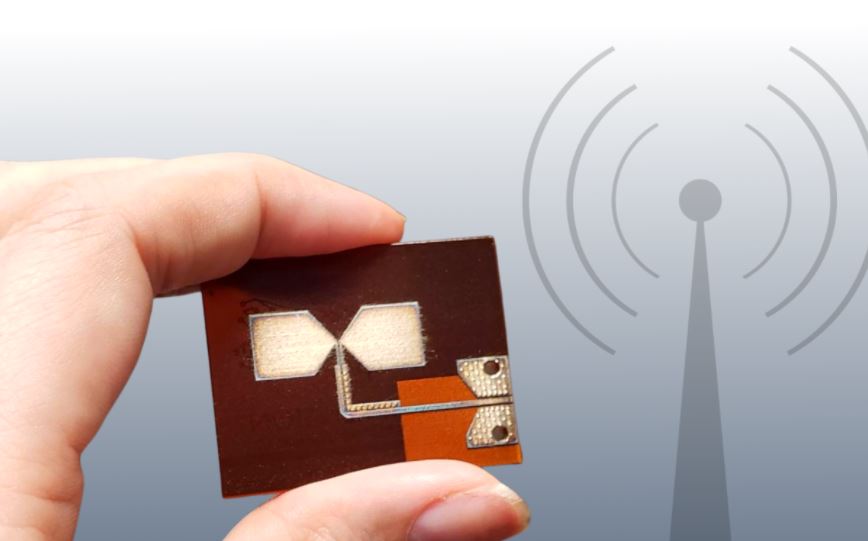
Speaking of IoT devices and the way they are produced, Storz states: “IoT devices are smarter and more connected. Due to their use of both analog and digital signals, designers need to follow certain guidelines in the design phase. There are devices that need to communicate, that’s why engineers will need to integrate wireless communication capabilities in their PCB. One way to do that is to embed an antenna and transceiver in the board.”
Printing conductive structures directly onto a substrate can help adapt antenna geometry. Integration with other components, RF tuning and testing remain necessary to obtain a functional device.
Low pass filter (LPF) devices are another interesting application that is worth noting. According to Storz, most common use of LPF devices is between RF transmission amplifier and the antenna. Therefore, it encounters widespread use in application such RF IoT devices and other RF communication devices.
Additive manufacturing of conductive and dielectric materials can combine some operations. It does not automatically perform every stage of a complete IoT device: component assembly, firmware, calibration and testing may remain separate.
“We did some tests to assess the performance and quality of 3D printed IoT devices we produce using our technology. We realized that 3D printed electronics provides exceptional results as the devices were higher than devices produced with other technologies and this performance was especially related to data transmission and quality. We learned that antennas that require a ground plane should be printed on multilayer boards, and that RF communications circuits/devices are one of the applications that will benefit the most from 3D printed IoT devices”, Storz concludes.
These results are reported by the supplier for its tests. The feature does not provide a comparative protocol establishing general superiority over all other processes.
Weight, cost and material suitability depend on the design and production route. Low outgassing, when required by the application, needs to be demonstrated for the materials and processing conditions used rather than assumed for all additively manufactured electronics.
In addition to prototyping new devices, and micro-manufacturing smart sensors, AM remains a good production candidate for IoT home devices. In the upcoming years, it will probably be complicated to list all the specific devices and sensors AM can help to produce.
Twikit emphasises starting with the application’s added value before choosing a technology, including for housings and part identification. “As always, we will first look at the added value of the application before deciding on which technologies to use. Projects have passed where casing of IoT devices were produced with AM, as well as a project where IoT was used for part identification in the AM process”, Joris concludes.

THE 3D ADEPT WEEKLY NEWSLETTER
The industry moves fast. Stay ahead.
Every week, the latest additive manufacturing news, in-depth features and real-world applications, straight to your inbox. Plus, be the first to know when a new issue of 3D ADEPT Mag is out.
Free · One email a week · Unsubscribe anytime
Clicking loads our email provider’s sign-up form, including its analytics and Google’s anti-bot protection. You’re only subscribed if you complete the sign-up. Read our privacy policy.