

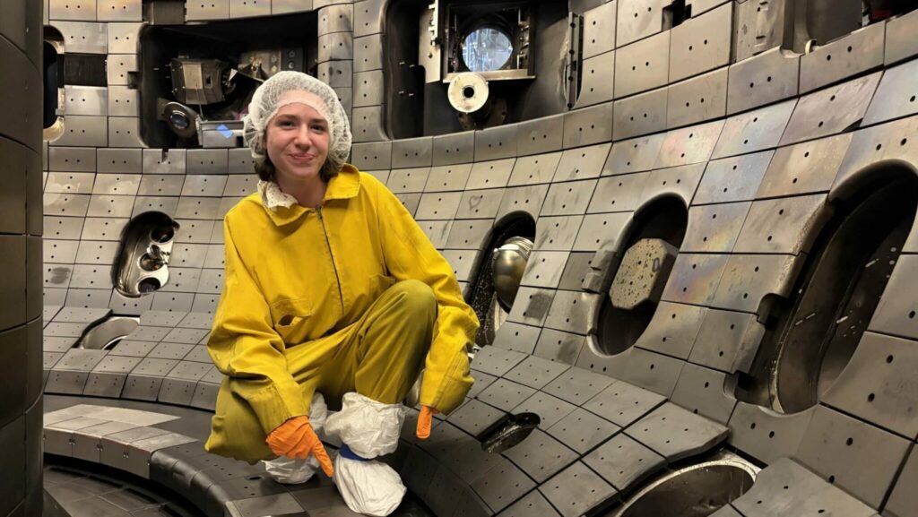
Researchers from North Carolina State University (NC State), Oak Ridge National Laboratory (ORNL) and Japan-based JEOL have put full-size 3D printed tungsten tiles inside a working fusion device. Installed in July 2026 in the lower divertor of the DIII-D National Fusion Facility in San Diego, the tiles went through 74 high-confinement (H-mode) discharges over three days. They came out intact, according to NC State.
“Tungsten is currently the material everyone wants in a fusion reactor,” says ORNL’s Michael Kirka, “but it is extremely difficult to manufacture into complex shapes.” The metal melts at 3,422 °C but is brittle at lower temperatures, and most tungsten printed with lasers comes out porous and cracked, NC State explains.
Additionally, plasma-facing parts in ITER and future fusion plants will have to withstand steady loads of 10 to 20 MW/m², more than 10,000 times direct sunlight.
From buttons to full-size tiles
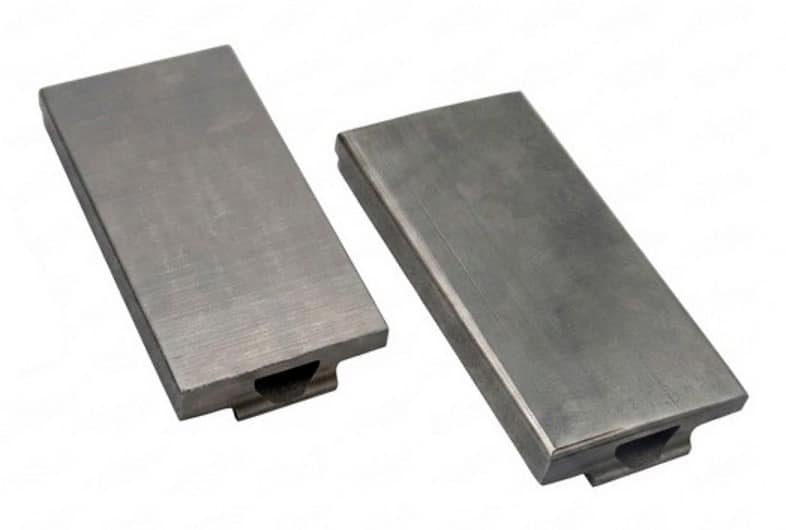
In 2025, tungsten buttons printed at NC State went through DIII-D’s Divertor Materials Evaluation System (DiMES) at heat fluxes near 20 MW/m², with peaks above 35 MW/m², and showed minimal damage. That result led Jonathan Coburn of Sandia National Laboratories to invite the team, in December 2025, to test a full-size tile.
It should be noted that a DIII-D tile measures about 140 x 130 mm, while the largest tungsten part NC State had produced so far was about 50 mm. JEOL stepped in with its large-format JAM-5200EBM electron-beam powder bed fusion (EB-PBF) system: flat and domed versions were printed in Akishima, Japan, over several iterations, with ORNL funding fabrication. NC State then shaped and ground them to a mirror-like finish.
“When DIII-D asked if we could do this, I said yes without blinking and then figured we’d have to sort out the details,” recalls Tim Horn, Associate Professor of mechanical and aerospace engineering and research director at the Center for Additive Manufacturing and Logistics (CAMAL) at NC State. “What we needed was the hardware and partners who could move fast. ORNL and JEOL were exactly that,” he adds.
Why electron beam additive manufacturing?
Remember when we reported, in 2024, that ORNL had produced the first defect-free complex tungsten parts with an electron-beam 3D printer? At the time, Kirka described electron-beam Additive Manufacturing as “promising” for complex tungsten geometries. It still is today: EB-PBF keeps the material above 1,400 °C during the build, hot enough for tungsten to avoid cracking.
During the DIII-D project, a misaligned tile next to the printed pair melted along its edge and spattered molten metal onto one of them. The printed tile survived that too according to the research team.
That said, going from small laboratory samples to a full-scale component in a tokamak within eight months is a major step toward validating the process.
THE 3D ADEPT WEEKLY NEWSLETTER
The industry moves fast. Stay ahead.
Every week, the latest additive manufacturing news, in-depth features and real-world applications, straight to your inbox. Plus, be the first to know when a new issue of 3D ADEPT Mag is out.
Free · One email a week · Unsubscribe anytime
Clicking loads our email provider’s sign-up form, including its analytics and Google’s anti-bot protection. You’re only subscribed if you complete the sign-up. Read our privacy policy.